


Research Programmes
[Summary by Dr. A. Tripathi and Dr. S. Ghosh (IIT Delhi). Updated by Dr. S. A. Khan]
Swift heavy ion irradiation results in many nonequilibrium processes including the formation of latent tracks and removal of atoms from the surface termed as electronic sputtering. The electronic sputtering study is one of the thrust areas of materials science research at IUAC. Sputtering process depends on a number of parameters including the electronic energy deposited in the system by ion beam, the crystallite grain size, conductivity of the material and properties of the substrate such as its conductivity. Due to the energy confinement in reduced dimensions in case of thin films and nano particles, the sputtering process is enhanced. Electronic sputtering is an important tool to understand the fundamentals of interaction of SHI with the matter and has been studied in detail in carbon allotropes, ionic crystals and many other materials at IUAC.
Electronic sputtering of different allotropes of carbon (diamond, graphite, fullerene, a-C and a-C:H) using using on-line elastic recoil detection analysis (ERDA) and catcher technique shows structure dependent sputtering yield of carbon from these allotropes. Hardest known allotrope diamond does not show any sputtering within the detection limit, whereas the soft polymerlike a-C:H shows highest sputtering yield (5.8x10⁵ atoms/ion). This significant variation of electronic sputtering yield of carbon in different allotropes is discussed from the viewpoint of influence of structure on ion–solid interaction [1]. The electronic sputtering study on fullerene (C60) thin films deposited on Si and glass substrates with Au and Ag ions of different energies. The velocity effect is shown to play an important role as slower ion having same electronic energy deposition (Se) as compared to its high velocity counterpart results in higher sputtering yield. Similarly films deposited on more insulating glass substrate shows higher sputtering yield as compared to those deposited on Si substrate. However, no charge state effect was observed in the electronic sputtering yield within the detection limit of the set up [2,3]. The angular distribution of sputtering from HOPG at different angles of incident and from amorphous carbon shows that the sputtering from HOPG is not isotropic and has been attributed to the crystal structure and formation of a thermal spike induced pressure pulse [4,5].
The sputtering from LiF thin films has been studied in detail. The sputtering yield of the order of 104 atoms/ion is measured and a reduction in sputter yield is observed with increasing grain size. It is explained that a smaller grain size leads to higher grain boundary scattering, lower mean diffusion length of the electrons leading to enhanced energy deposition inside the grains and increased sputter yield [6]. Similarly, a reduction in sputter yield to 2.2x10⁴ from 2.3x10⁶ atoms/ion, is observed with increase in the film thickness, which is attributed to the larger confinement of energy in the film having smaller grains and/or lower thickness [7]. Besides it is also shown that the sputtering yield increases exponentially with increasing lattice strain/crystal imperfections and materials with higher band gap show a higher sputtering yield. Electronic sputtering in CaF and CsI thin films by same group is also underway.
The sputtering studies on cupric nitride films deposited on borosilicate glass and Si substrates shows a 75% depletion of N whereas the copper content remains unchanged. The surface shows enhanced conductivity due to formation of nanodimensional metallic zones under Au ion impact [8]. The entire process is understood on the basis of thermal spike model of ion–solid interaction. Another important physical parameter which controls electronic sputtering yield is the band gap of the materials. It has been established in oxide that with higher band gap, the yield increases.
Two exponents for the size distribution of n-atom clusters, have been found in Au clusters sputtered from embedded Au nanoparticles under swift heavy ion irradiation and it is shown that the observed decay exponents do not support any possibility of a thermodynamic liquid-gas-type phase transition taking place, thus resulting in cluster formation [9]. Electronic sputtering studies of Zn embedded in silica showed that the sputtered species collected on carbon-coated transmission electron microscopy grids consist of Zn nanoparticles of sizes comparable to those present in the thin film [10].
Simulation work on electronic sputtering has also been reported to explain the large electronic sputtering yield [11]. Also, theoretical predication of sputter yield by the thermal spike simulation with refined parameters for nano-dimensional systems has been reported to have better agreement with the experimental values [12].
References
- S. Ghosh et al, Nucl. Instru. Meth. B219–220 (2004) 973–979.
- S. Ghosh et al, Nucl. Instru. Meth. B212 (2003) 431–435.
- S. Ghosh et al, Nucl. Instru. Meth. B190 (2002) 169–172.
- A. Tripathi et al, Nucl. Instru. Meth. B212, 402, (2003).
- A. Tripathi et al, Nucl. Instru. Meth. B266 (2008) 1265.
- M. Kumar et al, Nucl. Instru. Meth. B 256 (2007) 328–332.
- M. Kumar et al J. Appl. Phys. 102, 083510 (2007).
- S. Ghosh et al, Nucl. Instru. Meth. B 248 (2006) 71–76
- P.K. Kuiri et al, Phys. Rev. Lett. 100, 245501 (2008).
- C. Pannu et al., Beilstein Journal of Nanotechnology 5 (2014) 1691.
- S. Mookerjee et al, Phys. Rev. B78 (2008) 045435.
- U. B. Singh et al., J. Appl. Phys. 121 (2017) 095308.
[Updated by Dr. Fouran Singh]
The interaction of Swift Heavy Ions (SHIs) of energy ≥ 1MeV/nucleon with materials has enormous potential to modify their structure and thereby its properties. It is well established that these modification are the effect of energy loss by energetic ions, mainly by electronic energy loss (Se) process and dominates over second one which is nuclear energy loss (Sn) under high energy regime. Most of the previous work has shown that the ion irradiation produces damages, crystalline-to-amorphous and/or crystalline-to-crystalline phase transformation along their trajectories in many insulators/semiconductors where later processes have its dependence on certain threshold value of electronic energy loss. The effect of such high electronic energy deposition on transition metal oxides, semiconductors and metals induces the phase transformations of various kinds which have been extensively studied by utilizing the Tandem Pelletron Accelerator facility of IUAC New Delhi.
The phase transformation of orthogonal Ag2O3 into cubic Ag phase has been reported when sol-gel derived Ag2O3:ZrO2 films were irradiated with 100 MeV Ag ions at a fluence of ≥3×10¹² ions/cm2 [1]. Such phase transformation could be interesting for the evolution and tailoring of plasmonic properties in nanocomposites. In TiO2, though the thermal annealing is known to cause transformation from anatase to rutile phase in a temperature interval of 700–900 °C, a sizable volume fraction of anatase still remains. Irradiations by heavy ions on the other hand suppressed the anatase phase and almost phase pure rutile TiO2 could be obtained [2]. However, a irradiation of pure rutile phase exhibit amorphization through nano-crystallization [3] and the controlled annealing of these amorphous phase shows reversible phase transformations as well [4]. In spray pyrolysis derived thin films, transformation from metastable state to a different stable phase has been observed [5-7]. When irradiated with 100 MeV Ag ions, CdS thin films show a phase transformation from the metastable cubic to hexagonal phase. At the highest irradiation fluence, a significant amount of compressive strain is created in these films [5]. In polycrystalline CdTe films, transformation of the metastable hexagonal regions into stable cubic phase was also found [6]. In calcite single crystals, 120 MeV Au9+ ions irradiation induces the phase transformation from calcite to vaterite phases at fluences ≥5×10¹² ion/cm2 [8].
Zirconia is one of the very important materials in view of its applications and known to exhibit structural phase transformations upon variation in temperature and pressure such as monoclinic, tetragonal or cubic phases is the subject of intensive experimental and theoretical studies. Several studies on irradiations induced structural transformations along with their kinetics of transformation have been carried out [9-11]. The stability of yittria stabilized cubic zirconia has also been studied, including irradiation at high temperature [12-14]. Ion beam induced Cubic to Monoclinic Yttrium Oxide is also reported [15]. It is known that at high-temperature it has the cubic structure, which transforms to the tetragonal form at about 2570 K and at about 1400 K passes to the monoclinic phase. However, upon increasing in external pressure the monoclinic phase transforms into an orthorhombic phase. The tetragonal and cubic phases of Zirconia could be stabilized by extrinsic doping of yttrium. Apart from these reports, swift heavy ion irradiation induced phase transformations in ThGeO4 [16], YBa2Cu3O7−y thin films [17], ZnS nanocrystalline thin films [18].
References
- Manish Kumar, P.K. Kulriya, J.C. Pivin, and D.K. Avasthi, "Evolution and tailoring of plasmonic properties in Ag:ZrO2 nanocomposite films by swift heavy ion irradiation", J. Appl. Phys. 109 (2011) 044311.
- H. Rath, P. Dash, T. Som, P.V. Satyam, U.P. Singh, P.K. Kulriya, D. Kanjilal, D.K. Avasthi, and N.C. Mishra, "Structural evolution of TiO2 nanocrystalline thin films by thermal annealing and swift heavy ion irradiation", J. Appl. Phys. 105 (2009) 074311.
- S.K. Gautam et al, “Micro-Raman study on the softening and stiffening of phonons in rutile titanium dioxide film: Competing effects of structural defects, crystallite size, and lattice strain”, Journal of Applied Physics 115 (2014) 143504.
- S.K. Gautam et al “Reversible phase transformation phenomenon in titanium dioxide films: Evidence beyond interface-nucleation and dissolution-precipitation kinetics”, Acta Materialia 146 (2018) 253.
- V.V. Ison, A. Ranga Rao, V. Dutta, P.K. Kulriya, D.K. Avasthi, and S.K. Tripathi, "Swift heavy ion induced structural changes in CdS thin films possessing different microstructures: A comparative study", J. Appl. Phys. 106 (2009) 023508.
- V.V. Ison et al, "Swift heavy ion induced phase transition in CdTe films deposited by spray pyrolysis in presence of electric field", NIMB 267 (2009) 2480.
- P.K. Mochahari et al, “Structural phase transformation and modification of optical absorption of SHI induced nanostructured CdS films”, Journal of Materials Science: Materials in Electronics 29 (1), 582-588 2018.
- H. Nagabhushana et al, "Swift heavy ion irradiation induced phase transformation in calcite single crystals" Solid State Communications, 149 (2009) 1905.
- M. Rawat et al, “Micro-Raman and electronic structure study on kinetics of electronic excitations induced monoclinic-to-tetragonal phase transition in zirconium oxide films”, RSC Advances 6 (2016) 104425.
- H.S. Lokesha et al, “Evidence of luminescence modification with structure of zirconia phases”, Journal of Luminescence, 192 (2017) 173.
- Fouran Singh, “Micro-Raman investigations on zirconium oxide film during swift heavy ion irradiation to study crystalline-to-crystalline phase transformation kinetics by cascade overlap model”, Journal of Applied Physics 126 (2019) 025901.
- P Kalita et al, “Role of temperature in the radiation stability of yttria stabilized zirconia under swift heavy ion irradiation: A study from the perspective of nuclear reactor applications”, Journal of Applied Physics 122 (2017) 025902.
- R C Ramola et al, “Study of phase transformation induced by electronic excitation in pure and yttrium doped ZrO2 thin films”, Mater. Res. Express 4 (2017) 096401.
- P Kalita et al, “Investigating the effect of material microstructure and irradiation temperature on the radiation tolerance of yttria stabilized zirconia against high energy heavy ions”, Journal of Applied Physics 125 (2019) 115902.
- N.J. Shivaramu et al, “Ion beam induced cubic to monoclinic phase transformation of nanocrystalline yttria”, NIMB 379 (2016) 73.
- M.K. Patel et al, "Swift heavy ion induced structural modifications in zircon and scheelite phases of ThGeO4", NIMB 268 (2010) 42.
- R. Biswal et al, "200 MeV silver ion irradiation induced structural modification in YBa2Cu3O7−y thin films at 89 K: An in situ x-ray diffraction study", J. Appl. Phys. 106 (2009) 053912.
- S.P. Patel et al, "Structural phase diagram for ZnS nanocrystalline thin films under swift heavy ion irradiation", Physica B 406 (2011) 4150.
[updated by Dr. S. A. Khan]
Ion beam mixing is a phenomenon at interface between two layers, in which the atoms of one layer mingle with the atoms of the other elements under the influence of ion beam traversal through this. A low energy ion beam irradiation causes a ballistic mixing at the interface due to elastic collision cascades. The elastic collisions produce considerable defects in both the layers. These defects assist the diffusion across the interface, referred to as radiation enhanced diffusion. Since the energy lost by the ions in elastic collisions is called nuclear energy loss, therefore nuclear energy loss is considered to be responsible for ion beam mixing. It was later shown that the mixing at the interface could also be induced by the large electronic excitations of high energy heavy ions with the atoms in the sample. The striking feature of ion beam mixing is that (i) it has spatial selectivity, (ii) it is rather a low temperature process and (iii) thermodynamically immiscible systems, in principle, can be mixed.
Recently, single-phase CoSb3 fabricated by using low-energy ion irradiation of Co/Sb bilayer films and subsequent annealing was reported [1]. The Seebeck coefficient of these films of CoSb3 is found to be higher which has been attributed to the formation of a uniform layer of nanostructured CoSb3 alloy thin film. SHI-induced mixing studies on Ti/Bi system showed that mixing rate is higher for low-velocity Au ions in comparison to high-velocity Ag ions which could be due to less energy deposition in thermal spike by high-velocity ions [2]. Utilizing density functional theory (for calculating electronic specific heat and electron phonon coupling strength) and experimental results, it was recently shown that combination of the thermal spike model and the molten state diffusion is probably not sufficient to describe SHI mixing [3]
For a survey on electronic excitation induced ion beam mixing: Download (1.04 MB)
References
- Evolution of nanostructured single-phase CoSb3 thin films by low-energy ion beam induced mixing and their thermoelectric performance, M. Bala, S. Gupta, S. K. Srivastava, S. Amrithapandian, T. S. Tripathi, S. K. Tripathi, C.-L. Dong, C.-L. Chen, D. K. Avasthi, and K. Asokan, PCCP 19, 24886 (2017).
- Effect of ion velocity on SHI-induced mixing in Ti/Bi system, N. Bansal, S. Kumar, S. A. Khan, and R. S. Chauhan, Radiat Eff. Defects Solids 171, 290 (2016).
- Assessing a thermal spike model of swift heavy ion–matter interactions via Pd1−xNix/Si interface mixing, P. Patra, S. A. Khan, M. Bala, D. K. Avasthi, and S. K. Srivastava, PCCP 21, 16634 (2019).
Indra Sulania
Nanopatterns such as nanodots and nanoripples at various surfaces can be fabricated using energetic ion beams. Further, energetic ions upon incident on the surface, bring about the erosion of target atoms, mass displacement and re-deposition of the substrate materials. This kind of surface modification induced by incident ion beam is called ion beam sputtering (IBS). Nanopatterning at solid surfaces by ion beam sputtering (IBS) has been studied mostly for all kind of substrates especially semiconductors with an ion beam incident under a fixed sputter geometry at IUAC, new Delhi.
IUAC in-houses the facilities to provide (i) 1-1.5 keV wide beam (2 inch diameter), (ii) typically ~100 keV to 1 MeV positive ions of C, N, O, Ar, Kr etc. and negative metallic ions such as Au, Ag, Ti etc. and (iii) swift heavy ions (energies from 50 MeV to 200 MeV of Li, C, Si, Ni, Ag, Au, etc). All the above ion energy ranges have been extensively and effectively used for noteworthy results such as to obtained in synthesis of different nanocomposites materials and modifying the properties to use it in various applications.
References
- Topographic evolution of 500keV Ar4+ ion beam irradiated InP(100) surfaces formation of self-organized In-rich nanodots and scaling laws; I Sulania, D C Agarwal, M Kumar, S Kumar, P Kumar- Physical Chemistry Chemical Physics 18 (30) 2016, 20363-20370.
- Medium energy, heavy and inert ion irradiation of metallic thin films: studies of surface nanostructuring and metal burrowing: P Kumar, K Mal, S Kumar, I Sulania; Surface and Interface Analysis 48 (9) 2016, 969-975.
- Investigations of ripple pattern formation on Germanium surfaces using 100keV Ar+ ions; I Sulania, Agarwal, M Husain and D K Avasthi; Nanoscale research letters 10 (1) 2015, 88.
- Medium energy ion irradiationof Ge surface-search for better understanding of the surface nanopatterning; P Kumar, P Jain I Sulania - Surface and Interface Analysis 48 (4) 2016, 196-201.
- Role of surface composition in morphological evolution of GaAs nano-dots with low-energy ion irradiation; Tanuj Kumar, Manish Kumar, Govind Gupta, Ratnesh Kumar Pandey, Shammi Verma, and Dinakar Kanjilal; Nanoscale Research Letters, volume 7(1) (2012) 552.
- Tuning of ripple patterns and wetting dynamics of Si (100) surface using ion beam irradiation; Tanuj Kumar, Udai Bhan Singh, Manish Kumar, Sunil Ojha and Dinakar Kanjilal; Current Applied Physics, 14 (2014 312-317.
- Formation of nanodots on GaAs by 50 keV Ar+ ion irradiation; Tanuj Kumar, Udai Bhan Singh S Khan, S Verma, and Dinakar Kanjilal; Applied Surface Science; 258 (9) 2012, 4148-51.
- An approach to tune the amplitude of surface ripple patterns, Tanuj Kumar, Ashish Kuamr and Kanjilal, Appl. Phys. Lett. 103, 131604 (2013).
- Modification on CdS thin films due to low energy ion bombardment; I Sulania, D Agarwal, SK Tripathi and M Husain; Radiation Effects and Defects in Solids 167 (1) 2012, 59-68.
- Surface patterning on indium phosphide with low energy Ar atoms bombardment: an evolution from nanodots to nanoripples; I Sulania, A Tripathi, D Kabiraj, M Lequex and D K Avasthi; Adv. Mat. Lett; 2010, 118-122.
- Nano/micro-structuring of oxide thin film under SHI irraiation; RS Chauhan, DC Agarwal, S Kumar, SA Khan, D Kabiraj, I Sulania, Vacuum; 86(1) 2011, 96-100.
- Nano Pattern on n-Si (100) Surface by Ion Irradiation; Tanuj Kumar, S A Khan, U B Singh,, S Verma and D Kanjilal; AIP Conference Proceedings 1349 (2011) 727.
[ A Summary by A. Tripathi and D.K. Avasthi]
A brief survey of the research performed on ion beam synthesis and modification of carbon based nanostructures is given here.
1. Irradiation studies on Graphene and Synthesis of Au-graphene nanocomposite
Irradiation studies on Graphene is undertaken using swift heavy ions, low energy ions and electron beam. Commercially available 3-4 layer CVD grown graphene samples on Ni/Si/SiO2 were irradiated with 100 MeV Ag ions with fluences varying from 3×10¹⁰ to 3×10¹² ions/cm2. For each sample a mask of Al foil was used to cover half of the area. Raman spectra was taken at 4 different points on irradiated and pristine area of each sample. Average of each data was used in study. Raman data analysis shows decrease in Id/Ig ratio showing annealing effect of SHI in graphene at lower fluences. Graphene thin film were further irradiated with 60 MeV Ti,100 MeV Ag,150 MeV Au and 70 MeV O ion beams. Raman measurement showed only small annealing and no significant damage (e.g. in O beam irradiation) below a given threshold of electronic energy loss value. XRD (synchrotron) showed onset of damage at lower fluence at higher electronic energy loss values.
In-situ electrical measurement on single layer graphene (SLG) while irradiating with 100 MeV Ag ions showed decrease in resistivity at lower fluences, consistent with Raman and XRD results. Resistance of graphene layer decreases at lower fluences up to 3×10¹¹ ions/2 which is accompanied by the five-fold increase in electron and hole mobilities.
2. Au nano particle decorated on few layer grapheme
Au nano particles were deposited on few layer grapheme to make Au-graphene nanocomposite. With the help of Raman characterization, it has been observed that Au deposition on graphene produces strain in graphene samples and the strain increases with thickness of Au film. It has also been shown that after annealing of the Au decorated graphene samples at 400˚ C, strain is released as observed in XRD peak position shifting.
References
- Purification/Annealing of graphene with 100 MeV Ag ion irradiation, S. Kumar, A. Tripathi, S.A. Khan, F. Singh, V. Baranwal and D.K. Avasthi, Nanoscale Research Letters 9, 126 (2014).
- Engineering the strain in graphene layers with Au decoration, Compesh Pannu, Udai B. Singh, Sunil Kumar, A. Tripathi, D. Kabiraj, D.K. Avasthi, Applied Surface Science 308,193 (2014).
- Radiation stability of graphene under extreme conditions, Sunil Kumar, Ambuj Tripathi, Saif A Khan, Compesh Pannu and D K Avasthi, Applied Physics Letter 105, 133107 (2014)..
- Engineering of electronic properties of single layer graphene by swift heavy ion irradiation, Sunil Kumar, Ashish Kumar, Ambuj Tripathi, Chetna Tyagi and D K Avasthi, , Journal of applied Physics, 123, 16, 161533 (2017).
3. Annealing in SHI irradiated Graphene Oxide (Chetna Tyagi)
Graphene oxide films were irradiated by 120 MeV Au ions with different fluences of 3 × 10¹⁰, 1× 10¹¹, 3 × 10¹¹, 1 × 10¹², 3 × 10¹² and 1 × 10¹³ ions/cm2. The in-situ XRD results showed an increase in the crystallinity of film for lower fluence. The Raman spectra revealed the decrease in disorder parameter for lower fluences i.e. till 3×10¹¹ ions/cm2. Increase in graphitic region is indicated in FTIR spectra of GO for initial fluences. GO samples irradiated with high fluences.
4. Au-GO nanocomposites for Enzyme less glucose monitoring
Graphene oxide and its composites with gold nanoparticles were tested for glucose sensing applications. The Enzyme-less detection by Graphene oxide with gold nanoparticles (Au-GO) showed 25% more sensitivity towards glucose as compared to enzyme-immobilized Graphene Oxide electrode. This study also showed that the presence of gold nanoparticles played an important role in determining the sensitivity of the electrode. Electrode having higher percentage of gold nanoparticles showed better electrochemical properties as compared to the electrode having lower percentage of gold nanoparticles. Also, the selectivity is proved towards glucose among the common interfering agents, such as urea, cholesterol, Ascorbic acid, 4-acetaminophenol and citric acid. The low concentration (0.5:1) gold composites show better selectivity than the high concentration (10:1) gold composites. These electrodes show good storage stability for up to 15 weeks and hence make them suitable candidates for the application in glucose biosensors..
5. Voltammetric measurements of neurotransmitter-acetylcholine through metallic nanoparticles embedded 2-D material
Enzyme based AuNPs-GO (10:1) nanocomposite on ITO@ glass substrates as working electrode was prepared. Cyclic voltammetry curves showed the sensing ability of the working electrode towards Ach for a wide range of concentration varying from 100 pM to 1000 nM.. Interference studies showed the good selectivity of electrode for Ach among other common interfering agents and hence this electrode can be employed as rapid and precise Ach biosensor.
References:
- Structural changes in graphene oxide thin film by electron-beam irradiation, Chetna Tyagi, G.B.V.S. Lakshmi, Sunil Kumar, Ambuj Tripathi, D.K. Avasthi, Nuclear Instruments and Methods in Physics Research Section B Beam Interactions with Materials and Atoms, 379, (2016).
- Gold –graphene oxide nanocomposites for enzyme-less glucose monitoring, Chetna Tyagi, Lakshmi G. B. V. S., Veeru Jaiswal, Ambuj Tripathi, Devesh Kumar Avasthi. 08/2018; 4(6)., DOI:10.1088/2057-1976/aadd5f
- Investigation of graphene oxide-hydrogen interaction using in-situ X-ray diffraction studies, Chetna Tyagi, P.K. Kulriya, Sunil Ojha, D.K. Avasthi, Ambuj Tripathi: International Journal of Hydrogen Energy 06/2018; 43(29)., DOI:10.1016/j.ijhydene.2018.05.078
- Effect of carbon ion-beam irradiation on graphene oxide film, Chetna Tyagi, S.A. Khan, Sunil Ojha, D.K. Avasthi, Ambuj Tripathi: Vacuum 05/2018; 154., DOI:10.1016/j.vacuum.2018.05.003
- Evidence of Ion-Beam Induced Annealing in Graphene Oxide Film Using In-Situ X-ray Diffraction and Spectroscopy Techniques Chetna Tyagi, Saif Ahmad Khan, Indra Sulania, Ramcharan Meena, Devesh Kumar Avasthi, Ambuj Tripathi:. The Journal of Physical Chemistry C 04/2018; 122(17)., DOI:10.1021/acs.jpcc.7b10699
6. Modifications of the fullerene molecules (C60 and C70)
Studies of ion irradiation of C60 films show the formation of dimmer of fullerene (polymerization) [1-4] at low fluences and destruction of fullerene molecules at high fluences. The damage cross section of fullerene films under different Se has been studied [1,3,4].
The irradiation of fullerene thin film at low fluence by 90 MeV Si results in enhancement of PL emission. Most of the optical molecular transitions could be observed in PL in irradiated fullerene film [5]. The UV-Vis spectrum of the irradiated sample also revealed the molecular transitions, which were not so clear in the pristine sample.
Modifications of properties of C70 thin films following ion beam irradiation with 120 MeV Au ions have been investigated. The energetic ion impacts lead to the destruction of the C70 molecules. The radius ofdamaged cylindrical zone is about 2.9 nm [6]. A study on the comparision of behavior of C60 and C70under the SHI impingement indicates that C60 fullerenes form dimmer whereas C70 fullerenes do not form dimmer under SHI bombardment [7].
References:
- N. Bajwa, A. Ingale, D.K. Avasthi, R. Kumar, A. Tripathi, K. Dharamvir and V.K. Jindal. J. Appl. Phys. 94 (2003) 326.
- N. Bajwa et al., Radiation Measurements, 36 (2003) 737.
- N. Bajwa, A. Ingale, D.K. Avasthi, R. Kumar, A. Tripathi, K. Dharamvir and V.K. Jindal. J. Appl. Phys., 10 4 (2008) 054306.
- S. Lotha, A. Ingale, D. K. Avasthi, V. K. Mittal, S. Mishra, K. C. Rustagi, A. Gupta,and V. N. Kulkarni, D. T. Khathing, Solid. Stat. Comm., 111 (1999) 55.
- Amit Kumar, A. Podhorodecki, J. Misiewicz, D. K. Avasthi,and J. C. Pivin, J. App. Phys., 105 (2009) 024314.; Amit Kumar, F. Singh, R. Kumar, J. C. Pivin, and D.K. Avasthi, Sol. Stat. Comm. 138 (2006) 448.
- R. Singhal , Amit Kumar , Y. K. Mishra , S. Mahopatra , J. C. Pivin, D. K. Avasthi Nucl. Instr. and Meth. B 266 ( 2008) 3257.
- R. Singhal Amit Kumar, Y. K. Mishra, S. Mohpatra, J. C. Pivin, and D. K. Avasthi, Rad. Eff. and def. in Sol. 164 (2009) 38.
7. Ion beam synthesis of conducting nanowires
SHI irradiation of fullerene thin films at low fluence (1010 ions/cm2) results in the formation of conducting C nano wires embedded in fullerene matrix [1-3]. The conductivity of ion beam synthesized carbon nano wire is about 7 orders of magnitude more than the conductivity of virgin C60 film. The nanowires are parallel to each other and their length can be controlled by the thickness of fullerene film. The orientation of nanowires can be changed by simply changing the incidence angle of ion beam. As expected these nanowires like structure exhibits the field emission properties [3]. The formation of conducting C nanowires also occurs in SHI irradiation of DLC films [4-10].
The carbon nano-dot and nano-wires have also been synthesized using SHI irradiation of inorganic polymers/gels [6-10].
References:
- A. Tripathi, Amit Kumar, D. Kabiraj, S. A. Khan, V. Baranwal, D. K. Avasthi, Nucl.Instr. and Meth. B 244 (2006) 15.
- Amit Kumar, D.K. Avasthi, A. Tripathi, D. Kabiraj, F. Singh, J. C. Pivin, J. Appl. Phys. 101 (2007) 014308.
- Amit Kumar, L. D. Filip, J. D. Carey, D. K. Avasthi, J. C. Pivin, A. Tripathi, J. Appl.Phys., 102 (2007) 044305.
- J. Krauser, A.-K. Nix, H.-G. Gehrke, H. Hofsäss, C. Trautmann, A. Weidinger, F. Wünsch, J. Bruns, J. Vacuum Science Techn. B 26(2008)2468. ; J.Krauser, J.-H Jollondz, A. Wedeinger, C. Trautmann J. Appl. Phys. 94 (2003) 1959.
- Amit Kumar, F. Singh, J. C. Pivin, D.K. Avasthi, Journal of Physics D: Applied Physics 40,(2007), 2083.
- Amit Kumar, F. Singh, A. Tripathi J. Pernot, D. K. Avasthi, J. C. Pivin, Journal of Physics D: Applied Physics 41 (2008) 95304.
- S. K. Srivastava, D. K. Avasthi, E. Pippel, Nanotechnology, 17 (2006) 2518.
- Amit kumar, F. Singh, D. K. Avasthi, J. C. Pivin, Nucl. Instr. and Meth. B 244 (2006) 221.
- Amit Kumar, D. K. Avasthi, J. C. Pivin, Appl. Phys. Express 1 (2008)125002.
- Amit Kumar, D. K. Avasthi, A. Tripathi, F. Singh, I. Sulania, J. C. Pivin Journal of Nanoscience and Technology 7 (2007) 2201.
8. Ordering of Carbon Nanoubes by SHI irradiation
The experiments on SHI irradiation of CNT’s reveal that low fluence irradiation of carbon nanotubes results in the ordering of CNTs and destruction occurs at higher fluence [1]. The single-wall CNTs (SWCNTs) and multiwalled CNTs (MWCNTs) under irradiation of 55 MeV carbon ions show healing of CNTs under ion beam irradiation. The annealing process appears to begin at the lowest value of fluences and continues till the irradiation fluence of ~ 1x10¹⁴ ions/cm2 when the MWCNTs begin to amorphize whereas the SWCNTs continue to heal [2]. At low values of Se the defect annealing occurs till high fluences whereas the defect annealing at high Se values begins to vanish at lower fluence. Similar effects are observed for 120 MeV Au ion irradiation of multiwalled CNTs (MWCNTs)[28]. It is speculated that a narrow cylindrical region gets defects due to large energy density whereas in larger annular region surrounding it, the defect annealing takes place. The SHI irradiation results in Improvement in field emission properties of carbon nanotubes, diamond like carbon (DLC) films and nanocrystalline diamond film [3-8].
References:
- AmitKumar, D.K. Avasthi, J.C. Pivin and P.M. Konikar, Appl. Phys. Lett.92(2008)221904.
- KiranJeet, V.K. Jindal, L.M. Bharadwaj, D.K. Avasthi and Keya Dharmveer, Jl. Of Appl.Phys. 108 (2010) 034302
9. SHI induced Reorientation of Ni planes in Ni encapsulated by CNT
Reorientation of the crystalline planes occurs in nickel nanorods confined in CNT under SHI irradiation [1,2]. The effect of irradiation is dependent on the numbers of tube walls. The irradiation experiments show that the multi walled carbon nanotubes can be effectively used as radiation resistant coatings.
References:
- bha Misra, Pawan K. Tyagi, Padmnabh Rai, and D. S. Misra, Jay Ghatak, P. V. Satyam, and D. K. Avasthi, Appl. Phys. Lett. 89 (2006) 091907.
- Abha Misra, Pawan K. Tyagi, Padmnabh Rai, Dipti Ranjan Mahopatra, Jay Ghatak, P. V. Satyam, D. K. Avasthi, and D. S. Misra, Phys. Rev. B 76 (2007) 014108.
10. Defect mediated magnetism in Carbon Based Materials
The experimental findings based on SHI irradiation of fullerene films by Amit et al. [1-3] show that the magnetism in carbon based materials is mainly defect mediated. It was proposed the ferromagnetism in irradiated fullerene is due to some ordering of sp2 and sp3 bonded atoms having the correlation between unpaired spins and/or it could be related to the defects due to increase of O in the irradiated film.
References:
- Amit Kumar, D. K. Avasthi, J. C. Pivin, Appl.Phys. Express 1 (2008)125002.
- Amit Kumar, D. K. Avasthi, A. Tripathi, F. Singh, I. Sulania, J. C. Pivin Journal of Nanoscience and Technology 7 (2007) 2201.
- Amit Kumar, D. K. Avasthi, J. C. Pivin, A. Tripathi, F. Singh, Phys. Rev. B, 74 (2006) 153409
11. SHI induced modification of diamond thin films and nanostructures
The enhancement in the electron field emission in ultrananocrystalline and microcrystalline diamond films by SHI irradiation have been reported by Chen et al. It is observed that the local microstructure of the film changes drastically, without affecting the overall crystalline quality of the films. The enhancement is attributed to the formation of the interconnected nanoclusters network along the ion path and the enhancement is more prominent for microcrystalline as compared to nanocrystalline films.
References:
- Huang-Chin Chen, Umesh Palnitkar, Way-Faung Pong, I-Nan Lin, Abhinav Pratap Singh, and Ravi Kumar, J. Appl. Phys. 105, 083707 (2009).
12. Nanostructuring in other materials
Nano-structured materials have attracted much attention of researchers all over the world due to their extremely small size and large surface to volume ratio which led to size dependent chemical and physical properties, but different from their bulk counterparts. Ion beams can be used on various surfaces to engineer the size and shape of particles embedded in silica matrix. Some activities are initiated on possible applications as well as theoretical simulations. Energetic ions play significant roles in modifying these properties in materials science. Depending upon the mass and energy of the ion in question, various properties of the target materials gets modified. The role of energetic ions of energies from a few keV to hundreds of MeV in nanostructuring is explained with few examples of nanostructures obtained by ion irradiation experiments at Inter University Accelerator Centre (IUAC), Delhi.
The areas of research and investigations of ion beams in nananostructuring are as follows:
- Synthesis of nanostructures using low energy ion beams
- Study of the modifications of existing buried nanoparticles in a matrix so as to explore the possibility of engineering the size and shape of the nanostructures using high energy ion beams.
- Characterization using low and high energy ion beams
For a review of recent work in this field, please see. (1.17 MB)
(We gratefully acknowledge Current Science for giving permission to use the published work in this website).
Few Publications (2009-2011) in this area
Synthesis of nanostructured materials
- “Quasi-aligned gold nanodots on structured silica surface: Experimental and atomistic simulations investigations”, Saif A. Khan, Devesh K. Avasthi, Dinesh C. Agarwal, Udai B. Singh and Debdulal Kabiraj, Nanotechnology 22 (2011) 23530.
- “Engineering of hydrophilic and plasmonic properties of Ag thin film by atom beam irradiation”, Udai B. Singh, D.C. Agarwal, S. A. Khan, Manish Kumar, A. Tripathi, R. Singhal, B.K.Panigrahi, and D.K. Avasthi, Applied Surface Science 258 (2011) 1464–1469
- “Creation of Self organized gold nanostructures by keV ion beam irradiation”, U. B. Singh, D.C. Agarwal, S.A. Khan, A. Tripathi, Ajay Kumar, R. K. Choudhury, B.K.Panigrahi, and D.K. Avasthi, Radiation Effects and Defects in Solids 166 (2011) 553.
- “Nanopattern formation on n-Si(100) surface by ion irradiation” Tanuj Kumar, S. A. Khan, U. B. Singh, S. Verma and D. Kanjilal, , Solid State Physics, Proceeding of the 55th DAE Solid State Physics Symposium 2010, AIP Conference Proceedings, 1349 (2011) 727.
- “Synthesis of nanocrystalline α- Zn 2SiO 4 at ZnO-porous silicon interface: Phase transition study” R. G. Singh, Fouran Singh, R. M. Mehra, D. Kanjilal and V. Agarwal, Solid State Communications 151 (2011) 701.
- Synthesis of Au nanoparticles at the surface and embedded in carbonaceous matrix by 150 keV Ar ion irradiation. Jai Prakash, A. Tripathi, V. Riato, J. C. Pivin, Jalaj Tripathi, Keun Hwa Chae, Sanjeev Gautam, P. Kumar, K. Asokan, D.K.Avasthi , J. Phys. D: Appl. Phys. 44, 125302(2011).
- “Influence of mesoporous substrate morphology on the structural, optical and electrical properties of RF sputtered ZnO layer deposited over Porous silicon nanostructure”, Yogesh Kumar, J. Escorcia Garcia, Fouran Singh, S. Olive, V. V. Sivakumar, D. Kanjilal, V. Agarwal, Appl. Surface Science, (2011) doi:10.1016/j.apsusc.2011.09.131
- “Formation of nano dots on GaAs by 50 keV Ar + ion irradiation” Tanuj Kumar, S. A. Khan, U. B. Singh, S. Verma and D. Kanjilal, Applied Surface Science 2011 (in Press)
- “Growth kinetics of ZnO nanocrystallites: Structural, optical and photoluminescence properties tuned by thermal annealing” R. G. Singh, Fouran Singh, Vinod Kumar, R.M. Mehra, Current Applied Physics 11 (2011) 624.
- ‘Synthesis, characterization and thermal induced structural transformation in silver fullerene nanocomposite thin films for applications in optical devices, R. Singhal, D.C. Agarwal, Y.K. Mishra, D. Kabiraj, G. Mattei, J.C. Pivin, R. Chandra, D.K. Avasthi, J. of Appl. Phys. 107 (2010)103504.
- Surface patterning on indium phosphide with low energy Ar atoms bombardment: an evolution from nanodots to nanoripples; Indra Sulania, Ambuj Tripathi, D. Kabiraj, Matthieu Lequeux and Devesh Avasthi; Advance Material Letters, 1(2), 2010, 118-122
- Hydrogen induced lattice expansion and crystallinity degradation in palladium nanoparticles: Effect of hydrogen concentration, pressure, and temperature, Manika Khanuja, B. R. Mehta, Pragya Agar, P. K. Kulriya, and D. K. Avasthi, J. Appl. Phys. 106 (2009) 093515.
- Ge nanocrystals embedded in a GeOx matrix formed by thermally annealing of Ge oxide films, K.Vijayarangamuthu, S. Rath, D. Kabiraj, D. K. Avasthi, P.K.Kulriya, V.N.Singh, B.R.Mehta, Journal of Vacuum Science and Technology 27 (2009) 731.
- Nanoparticle-Induced Biodegradation of Poly( ε-caprolactone), Narendra K. Singh, Rathindra M. Banik, P K. Kulriya, Devesh K. Avasthi, Sudip Malik, and Pralay Maiti, Nanoscience and Nanotechnology Letters 1 (2009) 52.
- Radiation-resistant behavior of Poly(vinylidene fluoride)/Layered silicate nanocomposites, Vimal K. Tiwari, Pawan K. Kulriya, Devesh K. Avasthi, and Pralay Maiti, ACS Appl. Mater. Interfaces, 1(2) (2009) 311.
- Synthesis of plasmonic nanocomposite for diverse applications, D. K. Avasthi, Y. K. Mishra, R. Singhal, D. Kabiraj, S. Mohapatra, B. Mohanta, N. K. Gohil, N. Singh, Journal of Nanoscience and Nanotechnology, 9 (2009) 1.
- “White light emission from chemically synthesized ZnO–porous silicon nanocomposite” R G Singh, Fouran Singh, D Kanjilal, V Agarwal and R M Mehra, J. Phys. D: Appl. Phys. 42 (2009) 062002.
Modifications of nanostructured materials swift heavy ion
- Evolution and tailoring of plasmonic properties in Ag:ZrO2 nanocomposite films by swift heavy ion irradiation, Manish Kumar, P. K. Kulriya, J. C. Pivin, and D. K. Avasthi, Journal of Applied Physics 109 (2011)044311.
- “Softening of phonons by lattice defects and structural strain in heavy ion irradiated nanocrystalline zinc oxide films”, Fouran Singh, R. G. Singh, Vinod Kumar, S. A. Khan, and J. C. Pivin, J. Appl. Phys. 110 (2011) 083520.
- “Swift heavy ion interaction with silver–silica nanocomposites: an experimental surface plasmon resonance study”, Fouran Singh, J. C. Pivin, Doriana Dimova-Malisnovska, and J. P. Stoquert, J. Phys. D: Appl. Phys., 44 (2011) 325101.
- “Structural and spectroscopic modifications of nanocrystalline zinc oxide films induced by swift heavy ions”, Sebiha Rehman, R. G. Singh, J. C. Pivin, Waseem Bari, Fouran Singh, Vacuum, 86 (2011) 87.
- “Ionoluminescence studies of combustion synthesized Dy3+ doped nanocrystalline forsterite”, B.N. Lakshminarasappa, S.C. Prashantha, Fouran Singh, Current Applied Physics, 11 (2011) 1274.
- “Luminescence studies on swift heavy ion irradiated nanocrystalline aluminum oxide, K.R. Nagabhushana”, B.N. Lakshminarasappa, D. Revannasiddaiah, Fouran Singh, Journal of Luminescence, 131 (2011) 764.
- Nano/micro-structuring of oxide thin film under SHI irradiation R.S. Chauhan, D.C. Agarwal, S. Kumar, S.A. Khan, D. Kabiraj, I. Sulania, D.K. Avasthi and W. Bolse; Vacuum, Volume 86, Issue 1, 4 July 2011, Pages 96-100
- Study on synthesis of magnetic nanocomposite (Ni-Teflon) by swift heavy ion beam mixing, Jai Prakash, A. Tripathi, J. C, Pivin, Jalaj Tripathi, A. K. Chawla, R. Chandra, S. S. Kim, K. Asokan, D. K. Avasthi. , Adv. Mat. Lett. 2, 71(2011).
- Swift heavy ion-induced surface nanopatterning of indium oxide films, Neeti Tripathi, A. Tripathi, S. Rath Rad. Eff. and Def. in solids 166, 578(2011).
- “Enhancement of LPG sensing properties in nanocrystalline zinc oxide thin film by high electronic excitation”, Ravikiran B. Birajadar, Arindam Ghosh, Anil Ghule, Fouran Singh, and Ramphal Sharma, Sensors and Actuators B: Chemical, (2011) doi:10.1016/j.snb.2011.09.024\
- Enhancement of ferromagnetism in Pd nanoparticle by swift heavy ion irradiation, P. K. Kulriya, B. R. Mehta, D. K. Avasthi, D. C. Agarwal, P. Thakur,N. B. Brookes, A. K. Chawla, and R. Chandra, Applied Physicis Letters 96, (2010) 053103.
- Damaged carbon nanotubes get healed by ion irradiation, Kiran jeet, V.K. Jindal, L.M. Bharadwaj, D.K. Avasthi and K. Dharamveer, J. of Appl. Phys. 108(2010)034302.
- ‘Ion tracks in silica for engineering the embedded nanoparticles’, D.K. Avasthi, Y.K. Mishra, F. Singh, J. P. Stoquert, Nucl. Instr. and Meth. B 268(2010)3027.
- ‘Studies on carbon nanotubes under extreme conditions’, D.K. Avasthi, Amit Kumar, R. Singhal, A. Triapthi and D.S. Mishra, , J. of nanoscience and nanotechnology 10(2010)3767.
- Structural phase transformation in ZnS nanocrystalline thin films by swift heavy ion irradiation, Shiv P. Patel, A.K. Chawla, Ramesh Chandra, Jai Prakash, P.K. Kulriya, J.C. Pivin, D. Kanjilal and Lokendra Kumar, Solid State Communications, 150 ( 2010)1158.
- “Luminescence study of SHI irradiated nano semiconductor: conducting polymer composite” by S. Chowdhury, A.M.P. Hussain, G.A. Ahmed, F. Singh, D.K. Avasthi, A. Choudhury, Journal of Luminescence 130 (2010) 326.
- “Low temperature resistivity study of nanostructured polypyrrole films under electronic excitations” Subhash Chandra, S. Annapoorni, Fouran Singh, R.G. Sonkawade, J.M.S. Rana, R.C. Ramola, Nucl. Instrum. and Methods B 268 (2010) 62.
- Ion Beam Induced Modification of Metal Nanoparticles Dispersed Polymeric Films; Shah, Sejal; Singh, N. L.;Gavade, Chaitali;Shivakumar, V.;Sulania, Indra;Tripathi, A.; Singh, F;Avasthi, D. K.;Upadhyay, R. V.; Integrated Ferroelectrics, Volume 117,Number 1, 2010 , pp. 97-103(7)
- Swift heavy ion irradiation induced modification of the microstructure of NiO thin films, P. Mallick, Chandana Rath, Jai Prakash, D.K. Mishra, R.J. Choudhary, D.M. Phase, A. Tripathi, D.K. Avasthi, D. Kanjilal, N.C. Mishra , Nucl. Instru. and Meth. B 268, 1613-1617(2010)
- Poly(Vinylidene fluoride-co-hexafluoro propylene)/layered silicate nanocomposites: The effect of swift heavy ion, Vimal K. Tiwari, Pawan K. Kulriya, Devesh K. Avasthi and Pralay Maiti, J. Phys. Chem. B, 113 (2009)11632.
- Swift heavy ion induced modifications of optical and microstructural properties of silver-fullerene C60 nanocomposite, R. Singhal, D. C. Agarwal, Y. K. Mishra, S.Mohapatra, D. K. Avasthi, A. K. Chawla, R. Chandra and J. C. Pivin, Nucl. Instrum. and Meth. B 267(2009)1349.
- Electronic excitation induced tuning of surface plasmon resonance of Ag nanoparticles in fullerene C70 matrix, R. Singhal, D. C. Agarwal, Y. K. Mishra, F. Singh, J. C. Pivin, R. Chandra and D. K. Avasthi, J. Phys. D : Appl. Phys. 42(155103)2009.
- “Synthesis of silica: Metals nanocomposites and modification of their structure by swift heavy ion irradiation” J.C. Pivin, Fouran Singh, Y. Mishra, D.K. Avasthi, J.P. Stoquert, Surface & Coatings Technology, 203 (2009)2432.
- “Enhancement of field emission properties in nanocrystalline diamond films upon 100 MeV silver ion irradiation”, Huang-Chin Chen, Umesh Palnitkar, Balakrishnan Sundaravel, I-Nan Lin, Abhinav Pratap Singh, and Ravi Kumar, Diamond & Related Materials 18 (2009)164.
- “Shape deformation of embedded metal nanoparticles by swift heavy ion irradiation” Fouran Singh, S. Mohapatra, J.P. Stoquert, D.K. Avasthi, J.C. Pivin, Nucl. Instrum. and Method B 267 (2009) 936.
- “Perpendicular magnetization of FePt particles in silica induced by swift heavy ion irradiation” J C Pivin, Fouran Singh, O Angelov and L Vincent, J. Phys. D: Appl. Phys. 42(2009)025005.
- “Electronic excitations induced modifications of structural and optical properties of ZnO-porous silicon nanocomposites” R.G. Singh, Fouran Singh, I. Sulania, D. Kanjilal, K. Sehrawat, V. Agarwal, R.M. Mehra, Nucl. Instrum. and Methods B, 267 (2009)2399.
- “Modifications of structural, optical and electrical properties of nanocrystalline bismuth sulphide by using swift heavy ions” R.R. Ahire, Abhay A. Sagade, S.D. Chavhan, V. Huse, Y.G. Gudage, Fouran Singh, D.K. Avasthi, D.M. Phase, Ramphal Sharma, Current Applied Physics 9 (2009) 374.
- Studies of optical properties and SHI irradiation on PbS sensitized Nanoporous TiO2 network, Nabanita Dutta, Dambarudhar Mohanta, Indra Sulania and Amarjyoti Choudhury; Journal of Optics, Vol 38, Number 3 September 2009, pages 169-176
- VLS-like growth and characterizations of dense ZnO nanorods grown by e-beam process:, D C Agarwal, R S Chauhan, D K Avasthi, I Sulania, D Kabiraj, P Thakur, K H Chae, Amit Chawla, R Chandra, S B Ogale, G Pellegrini and P Mazzoldi; J. Phys. D: Appl. Phys. 42 035310 (2009)
- Surface roughness and power spectral density study of SHI irradiated ultra-thin gold films, P. Dash, P. Mallick, H. Rath, A. Tripathi, Jai Prakash, D.K. Avasthi, S. Mazumder, S. Varma, P.V. Satyam, N.C. Mishra, Applied Surface Science, 256, 558 (2009).
N.A. Shah1, P.S. Solanki1, Ramcharan Meena2, K. Asokan2
- Department of Physics, Saurashtra University, Rajkot – 360 005, India
- Inter University Accelerator Center, Aruna Asaf Ali Marg, New Delhi – 110 067, India
Present technology demands high quality devices which can be useful for high speed performance, high capacity of storage and low power consumption. A resistive switch is a two terminal device exhibiting an interesting hysteresis in current–voltage (I–V) characteristics [1]. Many oxide and non–oxide materials have been employed in the formation of resistive devices for their scientific study [2].
Every material exhibits distinguishable resistive switching (RS) behavior which can be generally classified into three different types, namely
- Unipolar switching
- Bipolar switching
- Threshold switching
Sometimes, combined unipolar and bipolar or unipolar and threshold switching behaviors are observed for few oxide materials [3].
The RS behavior can be understood in terms of
- Formation and rupture of filamentary paths
- Trapping and detrapping of charge carriers
- Migration of oxygen vacancies
In addition, it is worth to note that the RS behavior is strongly influenced by the top and bottom electrodes used. All these issues simultaneously create much confusion about proper understanding of the origin of RS behavior and its appropriate mechanism for various materials. In this context, till date, studies on RS behavior of, both, oxide and non–oxide materials are striking aspects of research for better spintronic based future device applications.
The RS effect is a most promising subject because of its potential applications in non–volatile memories [4]. This RS effect means device can be freely changed its own resistance states from high resistance state (HRS) or low resistance state (LRS) under the applied electric field. Recently, different kinds of oxide materials such as manganite, multiferroic and diluted magnetic semiconductor materials have been studied in detail for possible exhibition of RS effect [5].
The RS effect in oxide materials can be understood in terms of
- Formation and rupture of filamentary path
- Trapping and detrapping process of charge carriers
- Oxidation / reduction reaction
- Migration of oxygen vacancies
- Role of oxygen vacancies
The RS phenomenon has also been studied in–depth for mixed valent manganite based thin film devices [6].
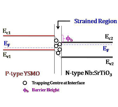
Among rare–earth manganites, YMnO3 (YMO) is one of the most studied multiferroic materials. Researchers have reported that YMO has, both, orthorhombic phase (o–YMO) and hexagonal phase (h–YMO). YMO manganite exhibits multiferroic behavior, i.e. coupling between magnetism and electricity (ferroelectricity). Electrical and magnetic properties have been studied well for YMO thin films [7]. Bogusz et al. [8] have studied bipolar resistive switching properties of pulsed laser deposition (PLD) grown YMO manganite layer grown on Nb:SrTiO3 (SNTO; 0.5 wt % Nb doping) substrate. They have discussed the RS in YMO/SNTO p–n junction on the basis of charge carrier density trapped / detrapped across the interface between YMO and SNTO. Wei et al. [9] have studied RS mechanism in PLD grown YMO/SNTO ferroelectric devices. The RS behavior with low power consumption observed in YMO/SNTO device has been explained in the context of electric field induced modifications in the width of depletion region at interface. The device exhibits a large RHRS / RLRS ratio, high endurance and long retention time.
Swift heavy ion (SHI) irradiation is one of the most important tools to create artificial defects, to modify the interface between film and substrate and to alter electrical and magnetic properties of oxide films. A foremost aim of the studies on SHI irradiation is to create artificial defects in the materials lattices in such a controlled way that these defects of the lattices improve some targeted properties specifically useful for some potential applications. Nanostructuring and creation of nanostructured defects modify almost all the properties of functional oxides including alterations in the oxygen ordering and content thereby all the properties of these oxides get altered in favor of potential applications. Several articles are available on the SHI studies for various functional oxides for their structural microstructural, electrical, transport, magnetoresistance and magnetic properties [10-19].
By considering all these aspects of various oxides, functional oxide materials, manganites, YMnO3 based perovskites and SHI irradiation, in last four years, we have attempted to study the RS behavior of pristine lightly doped YMnO3 manganite films (i.e. Y0.95A0.05MnO3; A = Ca and Sr), grown using pulsed laser deposition (PLD) method on single crystalline Si and Nb:SrTiO3 (SNTO) substrates, along with their responsible conduction mechanisms. This has been followed by performance of SHI irradiation on all these films with various ion fluence and same RS behavior with possible mechanisms have been studied well. Work has been published in some reputed journals as well as (till date) communicated to some good journals for publication. Following are some interesting results published in three different research journals in last year, i.e. 2019 [20-22].
|
1. Keval Gadani et al Journal of Alloys and Compounds 788 (2019) 819–830: [Ref-20] SHI Irradiation Effects on RS behavior of Y0.95Sr0.05MnO3 / SNTO Manganite Films Film Thickness: 100nm Ions: 200MeV Ag+15 Fluence: 1E11, 1E12, 1E13 |
|
|
|
|
|
| 2. Bharavi et al Thin Solid Films 685 (2019) 151–160: [Ref. 21] SHI Irradiation Effects on RS behavior of Y0.95Sr0.05MnO3 / SNTO Manganite Films Film Thickness: 300nm Ions: 200MeV Ag+15 Fluence: 1E11, 1E12, 1E13 | |
|
|
|
|
| 3. Kunalsinh et al Physica Status Solidi B 256 (2019) 1900264: [Ref:22] SHI Irradiation Effects on RS behavior of Y0.95Sr0.05MnO3 / Si Manganite Films Film Thickness: 100nm Ions: 200MeV Ag+15 Fluence: 1E11, 1E12, 1E13 | |
|

|
|
|
References
- Chua et al, Semicond. Sci. Technol. 29 (2014) 104001
- Ye et al, J. Mater. Sci. Technol. 32 (2016) 1.
- Lee et al, Appl. Phys. Rev. 2 (2015) 031303.
- Yang et al, Nature Nanotechnol. 8 (2013) 13.
- Chen et al, Adv. Mater. 24 (2012) 3515.
- Li et al, J. Appl. Phys. 105 (2009) 143110.
- Li et al, Appl. Phys. A 94 (2009) 975.
- Bogusz et al, Nanotechnology 27 (2016) 455201.
- Wei et al, RSC. Adv. 6 (2016) 1445.
- Vaghela et al, Phys. Chem. Chem. Phys. 19 (2017) 5163.
- Ravalia et al, J. Appl. Phys. 116 (2014) 153701.
- Ravalia et al, Ind. J. Phys. 89 (2015) 137.
- Shibuya et al, Adv. Mater. 22 (2010) 411.
- Joshi et al, J. Appl. Phys. 105 (2009) 073704.
- Bhavsar et al, Radiat. Eff. Defects Solids, 166 (2011) 718.
- Okada et al, Jpn. J. Appl. Phys. 53 (2014) 05FB10.
- Polek et al, Nanoscale Res. Lett. 12 (2017) 180.
- Polek et al, Superlattice Microstruct. 120 (2018) 525.
- Gadani et al, Mater. Today Proc. 5 (2018) 9916.
- Keval Gadani et al Journal of Alloys and Compounds 788 (2019) 819–830.
- Bharavi et al Thin Solid Films 685 (2019) 151–160:
- Kunalsinh et al Physica Status Solidi B 256 (2019) 1900264
[Summary by Dr. Fouran Singh]
Wide band gap materials are the field of immense research interest not only due to their potential applications in harsh environment, but also to understand various interesting phenomenon [1-3]. Large varieties of the WBG materials have been investigated for modifications in their properties by swift heavy ion (SHI) irradiation at IUAC, such as Oxides [3-27], Nitrides [28-30], and Carbides [31]. The brief discussions are given in following sections.
1. Semiconducting oxide thin films and nanostructures
Among the oxide semiconductors, ZnO based thin films and nanostructures have been investigated extensively for the surface, structure, optical, luminescence, transport, and phonon structure modifications by SHI irradiations [2-15]. SHI induced surface nanostructuring studies on sputtering and evaporation grown ZnO thin film have shown that this technique can be used very effectively to modify the properties of ZnO thin film [7-10]. Studies have also shown defects induced local amorphization along with modifications in transport properties [11-14] and growth of quantum dots [16] by SHI irradiation on thin films grown by chemical route ZnO films. It is reported that the stress in the ZnO crystallites can be controlled and is very useful in understanding the phonon structure in depth [4]. The studies have also shown that SHI irradiation is very efficient in the development of ZnO based materials for gas sensor [14] and spintronic [15] applications.
Phase transition in TiO2 thin films from anatase to rutile in chemically grown films in chemically grown nanocrystalline films [16] is reported. While in other studies on sputtering films (grown by sputtering process), a phase transition to rutile and brookite along with ferromagnetism at room temperature by SHI irradiations are also reported [18]. The studies also reported an amorphization through nanocrystallization induced by ion irradiation, including the reversible phase transformation [20]. It is also shown that Fermi level can be shifted by dense electronic excitations induced by SHI irradiation, which is very crucial parameter in the development of photodiodes and it stability under irradiation [20]. It is also reported that the photo-electrochemical response of TiO2 films can be improved by SHI irradiation [17]
SHI can induce formation of nanoparticles by the phase separation in indium sub-oxide films and on the surface In2O3 thin films [22], along with s significant morphological changes. However, films annealed in oxygen shows clusters of In2O3 phase induced by thermal annealing and studies have shown that such clusters can be dissolved by ion irradiation [23]. The modifications in structural and transport properties [24], bad gap engineering [25] under irradiations has also been reported. The nanocrystallization of PLD grown thin films of SnO2 and the enhancement of the gas sensing properties by SHI has also been reported [26]. It has also been observed that the nature of sensing is changed from n-type to p-type after the irradiation. The modifications in the properties of nanocrystalline cadmium oxides by virtual gap states and their correlation with p-d hybridization, anomalous enhancement of the bandgap and even the phase transformation from rocksalt to wurtzite has also been reported [27].
2. Nitride thin films and nanostructures
The pure and Co implanted MOCVD grown epilayer has been irradiated by SHI irradiations for the modifications in the structural, optical, photoluminescence and transport properties [28-30]. The PL and PL excitations studies have shown that band-to-band emission disappears by SHI irradiation and the deep level defects induced yellow emission also observed to be getting modified [28]. The recovery of blue emission by thermal annealing has also been observed in this study. The studies have also shown that SHI irradiation induced compressive strain in the lattice along with broadening in the band edge absorption [29]. The damage in the epilayer has been understood by the loss of Nitrogen induced by dense electronic excitations. In other study of Co-doped GaN for diluted magnetic semiconducting applications; it is observed that RTA at 1150 °C for 20 s is the most effective annealing process in comparison to the ion irradiation process [30]. But, the cluster formation could not be observed after the treatment of RTA and SHI irradiation both.
3. SiC nanostructures
A comparative study on buried SiC layers have been carried for the modifications in the structural properties by thermal annealing and athermal annealing by SHI irradiation [31]. This study has shown that annealing induces the formation of SiC crystallites in the near surface region of C-implanted Si, but the irradiation by 110 MeV Ni ions have not been able to induces significant re-crystallization of SiC.
References
- U. Ozgur et al, J. Appl. Phys. 98, 041301-1 (2005).
- R.G. Singh et al, J. Phys. D: Appl. Phys. 42/FTC, 062002 (2009).
- Ravikiran B. Birajadar et al, Sens. Actuators B 160, 1050 (2011).
- Fouran Singh et al, J. Appl. Phys. 110 (2011), 083520; ibid N. Gautam et al, Physica B 570, 13 (2019).
- S. Rehman et al, Vacuum 86, 87 (2011).
- S.K. Neogi et al, J. Phys.: Condens. Matter 23, 205801 (2011).
- Fouran Singh et al, Solid State Commun. 150, 1751 (2010).
- R.G. Singh et al, Nucl. Instru. and Method B 267, 2399 (2009).
- D. C. Agarwal et al, Surf. & Coat. Tech. 203, 2427 (2009); ibid Scientific Reports 9, 6675 (2019).
- V.V. Sivakumar et al, Appl. Surface Science 317, 1075 (2014).
- V. Kumar et al, J. Alloy & Compounds 544, 120 (2012); ibid Appl. Surface Science 279, 472 (2013); ibid Himanshi Gupta et al, Phys. Chem. Chem. Phys. 21, 15019 (2019).
- Y. Kumar et al, Appl. Surf. Science 258, 2283 (2012); ibid Nanoscale Research Lett. 7, 366 (2012).
- Fouran Singh et al, J. Appl. Phys. 112, 073101 (2012); ibid S.K. Gautam et al, Solid State Communications 218 (2015) 20-24.
- S. Ranwa et al, IEEE Sensors Journal 62, 7586 (2016); Ibid Journal of Applied Physics 115, 233706 (2016); ibid Applied Physics Letters 105, 213103 (2016).
- P. Sen et al, J. of Magnetism and Magnetic Materials 385, 318 (2015).
- H. Rath et al, J. Appl. Phys. 105, 074311 (2009).
- A. P. Singh et al, J. Phys. Chem. C 114, 622-626 (2010).
- Hardeep Thakur et al, Appl. Phys. Lett. 98, 192512 (2011); ibid J. Appl. Phys. 110, 083718 (2011).
- Avesh Kumar et al, Appl. Phys. Lett. 99, 013109 (2011).
- S.K. Gautam et al, J. Appl. Physics 115, 143504 (2014); ibid Acta Materialia 146, 253 (2018).
- S.K. Gautam et al, Phys. Chem. Chem. Phys. 18, 3618 (2016); ibid J. Appl. Phys. 120, 214502 (2016); IEEE Trans. Electron Devices 66, 1475 (2019).
- Neeti Tripathi et al, NIMB 268, 3335 (2010).
- S.K. Gautam et al, Ceramics International 42 (2016) 2846.
- MPS Rana et al, Thin Solid Films 616, 34 (2016).
- MPS Rana et al, (2016) Ceramics International, 42, 5932 (2016).
- P. Tyagi et al, NIMB 379, 219 (2016)
- A. Das et al, Scientific Reports 7, 40843 (2016); ibid Vacuum 10, 146 (2017); ibid Nanoscale 11, 14802 (2019); ibid Nanoscale 12, 669 (2020).
- G. Devaraju et al, Nucl. Instrum. and Methods B 269, 1925 (2011).
- V. Suresh Kumar et al, Physica B 406, 4210 (2011).
- Ashish Kumar et al, Materials Research Express 3, 085901 (2016); ibid Appl. Phys. Lett. 111, 222102 (2017); ibid J. Appl. Phys. 123, 161539 (2018); ibid Semiconductor Science and Technology 33, 085008 (2018); Materials Science and Engineering: B 186, 89 (2014).
- Y. S. Katharria et al, J. Appl. Phys. 105, 014301 (2009).
[A Summary by Dr. P.K.Kulriya]
Research on the energy material is important to fulfil the increasing demand for clean energy having a low-carbon footprint. Among the all types of energy sources, nuclear energy accounting for nearly 3 % of electricity generation in India which is expected to increase due to commissioning of a large number of nuclear power plants. There are few challenges associated with nuclear energy like extension of the life of existing nuclear power plants, utilization of thorium as a fuel, compact nuclear reactors, storing, recycling and safe disposal of the spent nuclear fuel in which materials science can play key role. Because of this pivotal importance of materials in view of sustainable nuclear energy, a research programme on the materials for nuclear energy applications is started at IUAC. The main aim of the programme is to develop radiation-resistant ceramic and metallic alloys and their performance evaluation under extreme condition like high temperature, prolonged irradiation, and chemically hostile environments. Irradiation studies on the nuclear materials suggest that energetic ions can lead to volume swelling, pores, micro-cracks, grain coarsening and a wide variety of point defects, which leads to phase transformation and/or amorphization of the materials. These changes are strongly depending upon the energy of incident ion, the mass of the incident ion, ion fluence, and temperature of the target. In collaboration with researchers from various universities and institutes, irradiation studies have been carried out on ceramic waste form namely pyrochlore [1-5], zirconolite [6-7], orthophosphate monazite [6] and surrogate nuclear materials like zirconia [7], ceria and zircon type ThGeO4, etc.
Ceramic waste form
Ceramics materials such as pyrochlore A2B2O7, zirconolite CaZrTi2O7, zircon ZrSiO4, monazite (La, Ce, Nd) PO4 and other complex oxide having high waste loading capacity, better thermal, mechanical, natural analogous and desired chemical properties are proposed as potential materials for the immobilization of high-level nuclear waste [HWL] as well as a waste form for accelerator-driven subcritical systems. Among these ceramic materials, the pyrochlore structure shows immerse applications as nuclear waste forms, and inert fuel matrix for incorporating radionuclides due to its better radiation-resistant response. In addition, some of the pyrochlores have potential to be used as a burnable neutron poisons in nuclear reactors. Isometric pyrochlore A2B2O7 (where cation A can be lanthanide, Y, actinides and cation B can be Ti, Zr, Hf, Sn) is a superstructure of the ideal defect fluorite structure. It displays capability for storage and transmutation of actinides (e.g., U, Np, Th, Pu, Am, and Cm) at the A-site and tunable chemical properties by changing the composition of A- and B- site cations. High-temperature irradiation which can able to maintain a temperature of 1000 oC during swift heavy ion irradiation is installed in the materials science beamline at superconducting LINAC accelerator [5]. Temperature-dependent swift heavy ion irradiation studies on Nd2Zr2O7, Gd2Zr2O7 and Gd2Ti2O7 pyrochlores showed that the ion track is created due to SHI irradiation and size of ion track critically depends upon the temperature and ion fluence. The in-situ X-ray diffraction (XRD) along with micro-Raman spectrometric analysis on Nd2Zr2O7 irradiated at 300 K displayed order-disorder phase transformations. Temperature-dependent irradiation studies revealed a slow rate of degradation at elevated temperature due to the competition in between defect production and thermal healing mechanism. Effect of size of cation on the irradiation showed that Gd2Zr2O7 is better radiation tolerance than Nd2Zr2O7. Furthermore, it is also observed that titanates can be readily amorphized, whereas zirconate pyrochlore exhibits better radiation tolerance [1-5]. Irradiation studies have been also carried out on another potential waste form namely zirconolite. Single-phase zirconolite samples are synthesized using conventional two-step solid-state technique by mixing the oxide powders CaCO3, ZrO2 and TiO2 in their stoichiometric ratios. Single-phase zirconolite samples are irradiated with 120 MeV Au9+ ions different ion fluence varied from 1×10¹¹ ions/cm2 to 1×10¹⁴ ions/cm2. In-situ XRD studies on the irradiated samples showed that initially, the crystallinity of the CaZrTi2O7 is found to lose by the loss of diffraction peaks and appearance of broad amorphous bands in XRD patterns which eventually lead to amorphization at higher ion fluence. Amorphization trend with fluence also indicates the formation of ion tracks that overlap at still higher fluences further affecting the irradiated area. Swift heavy ions also produce damage in terms of the formation of defects/vacancies and induced strains that result in an increase in spacing between the atoms by displacing them from their ideal crystalline positions. As a consequence, lattice expansion is noticed while increasing ion fluence which is confirmed by the negative peak shift in XRD patterns. Due to the large gap between atoms along (001) axis in pristine form, defects/vacancies prefer to occupy the free space and hence, there appears to be an expected lattice expansion along (001) axis. Maximum expansion is however observed for parameter ‘b’ than ‘c’. Further, the irradiation-induced displacements of atoms lead to distortion of bonds as also confirmed through peak intensity reduction in Raman spectra and the observed new broad peak in the spectra at higher fluences indicates amorphization of material. Moreover, the formation of TiO5 is expected due to bond distortion of octahedral TiO6, which becomes a key factor in determining the stability of zirconolite even in the amorphized state. Besides amorphization, some crystalline part of zirconolite is found to be present even at the highest fluence available (1×10¹⁴ ions/cm2) as observed both through XRD and Raman spectroscopy measurements yielding incomplete overlap of amorphized ion tracks. Thus, the presence of the residual crystallinity makes zirconolite (CaZrTi2O7) a better radiation resistance compound than pyrochlore under high energy regime [9-11].
Surrogate nuclear materials:
Understanding the behavior of nuclear fuels and cladding materials during the operation of nuclear reactors is crucial to the safety of the nuclear power plant and the enhancement of fuel performance. But, studying irradiated fuel (UO2, PuO2), is extremely challenging and hazardous. Due to these limitations, there is an increasing interest in using surrogate materials like zirconia, ceria, to complement the post-irradiation examination of nuclear fuel. We have investigated the effect of microstructure and target temperature on the radiation tolerance against high electronic energy loss (80 MeV Ag6+) in the ceria and yttria-stabilized zirconia. X-ray diffraction along with Raman spectroscopy measurements showed that the nano-crystalline samples suffered more damage as compared to the bulk-like sample irrespective of the irradiation temperature. Similar results were also observed in the case of ceria. A reduction in the irradiation damage i.e. improvement in radiation tolerance was also observed for all the samples irradiated at elevated temperature. Our study clearly established that irradiation damage, against Se, is critically dependent on the interplay between the irradiation temperature and crystallite size [12-13].
References:
- Probing the temperature effects in the radiation stability of Nd2Zr2O7 pyrochlore under swift ion irradiation, Saurabh Kumar Sharma, V Grover, AK Tyagi, DK Avasthi, UB Singh, P K Kulriya, Materialia 6(2019) 100317.
- Investigations of atomic disorder and grain growth kinetics in polycrystalline La2Zr2O7, Asha Panghal, Pawan K Kulriya, Yogendra Kumar, Fouran Singh, N L Singh, Applied Physics A 125(2019) 428.
- Influence of grain growth on the structural properties of the nanocrystalline Gd2Ti2O7, P K Kulriya, Tiankai Yao, Spencer Michael Scott, Sonal Nanda, Jie Lian, Journal of Nuclear Materials, 487 (2017) 373-379.
- Radiation stability of Gd2Zr2O7: Effect of stoichiometry and structure, Renu Kumari, P. K Kulriya, V. Grover, R. Shukla, K. Saravanan, S. Mohapatra, A. K Tyagi, D. K. Avasthi, Ceramics International 42 (2016) 103-109.
- In-situ high-temperature irradiation setup for temperature-dependent structural studies of materials under swift heavy ion irradiation, P K Kulriya, Renu Kumari, Rajesh Kumar; V Grover, R. Shukla, A K Tyagi, D K Avasthi, Nucl. Instr. and Meth. B 342(2015) 98.
- Reduction and structural modification of zirconolite on He+ ion irradiation, Merry Gupta, P K Kulriya, Rishabh Shukla, R S Dhaka, Raj Kumar, SS Ghumman, Nuclear Instruments and Methods in Physics Research Section B: Beam Interactions with Materials and Atoms 379(2016)119-125.
- Phase analysis and reduction behaviour of Ce dopant in zirconolite, Rajveer Kaur, M Gupta, P K Kulriya, SS Ghumman, Journal of Radioanalytical and Nuclear Chemistry (2019) 1-10.
- Probing swift heavy ion irradiation damage in Nd-doped zirconolite, Merry Gupta, P. K. Kulriya, R. C. Meena, S. Neumeier, S. S. Ghumman, Nucl. Instr. and Meth. B 453(2019)22-27
- Structural response of Nd stabilized zirconia and its composite under extreme conditions of swift heavy ion irradiation, Chiranjit Nandi, V Grover, P. K Kulriya, A. K. Poswal, Amrit Prakash, K. B. Khan, D. K. Avasthi, A. K. Tyagi, Journal of Nuclear Materials 499 (2018) 216-224
- Parswajit Kalita, Santanu Ghosh, Gaël Sattonnay, Udai B Singh, Vinita Grover, Rakesh Shukla, S Amirthapandian, Ramcharan Meena, AK Tyagi, Devesh K Avasthi, Journal of Applied Physics 122 (2014)025902
- Effect of grain size and microstructure on radiation stability of CeO2: an extensive study, V Grover, R Shukla, R Kumari, B P Mandal, P K Kulriya, S K Srivastava, S Ghosh, A K Tyagi, D K Avasthi Physical Chemistry Chemical Physics 16(2014) 27065-27073
- Swift heavy ion induced structural modifications in zircon and scheelite phases of ThGeO4, M. K. Patel, D. K. Avasthi, P.K. Kulriya, S. Kailas, J.C. Pivin, A. K. Tyagi, V. Vijayakumar, Nucl. Instr. and Meth. B 268(2010) 42
Understanding Ion beam induced recrystallization
Anusmita Chakraborty, Debdulal Kabiraj
When an energetic ion beam is incident on a target, the slowing down of ions in the target material is separated into two distinct processes: Elastic/Nuclear energy loss (Sn) and Inelastic/Electronic energy loss (Se). The energy (Sn) lost by the incoming ion that is transferred to the recoiling target nucleus can be thought of as being elastic scattering of two screened heavy particles. This process is responsible for the production of lattice disorder and most of the damage to the crystal structure of the target material. It dominates at low energy and atomic movements are anticipated. Whereas, the inelastic energy (Se) lost by the incident ions is dissipated through the electron cloud into lattice phonons (vibrations) of the target material. For high energy heavy ions (MeV to GeV), often called ’Swift heavy ion (SHI)’, Se is sometimes two orders higher in magnitude than Sn and no atomic movement is expected in this regime. Before understanding ion beam induced recrystallization, it is essentially important to consider the processes involved in thermal annealing leading to recrystallization. At elevated temperatures, instantaneous recombination of interstitials and vacancies is enhanced and defects become more mobile whereas, at low temperatures mobility of defects is reduced. In partially damaged layers, recovery occurs throughout the layer but for completely amorphous layers, recrystallization occurs at the amorphous-crystalline (a-c) interface as the buried crystalline region provides the necessary platform for recovery.
To observe recrystallization in the low energy regime, there is a threshold that has a dependence on the combination of irradiation temperature and production of atomic displacements due to nuclear energy (Sn) deposition around the crystalline/amorphous interface. Low-energy ions whose projected ranges are smaller than the initial amorphous layer have been observed to induce crystallization in GaAs. Channeling-Rutherford Backscattering (C-RBS) spectra representing ion beam induced epitaxial recrystallization (IBIEC) of the As/N implanted layer in GaAs has been observed using low energy Ar and Kr at temperatures lower than thermal annealing [1-3]. When thermal annealing of the a-SiC layers is performed above 950°C, recrystallization is found resulting in a highly defected crystalline structure [4]. In the nuclear energy loss regime, the IBIEC effect is observed at lower irradiation temperature in pre-implanted 6H-SiC samples after irradiation at 480 °C with 300 keV Si ions and at 600 °C with 3 MeV Ge ions [5-6].
Moving to the electronic energy loss regime, irradiation of materials with SHIs is expected to cause no atomic displacements and low energy ions are needed to achieve desirable atomic displacements. On the contrary, observations show structural modifications including deformations, amorphization and recrystallization even in case of interaction of SHIs with materials [7-18]. Often it has been observed that when SHIs are incident on a material target, highly defective or amorphous structures are created within the material under certain conditions. The ion trajectories in the material are known as latent ion tracks [19-20]. The explanation for track formation is based on the Thermal Spike Model (TSM) that considers the transfer of Se by electron-phonon interactions from the electronic subsystem to the atomic subsystem of the target atoms leading to a local thermal spike rising the lattice temperature and providing sufficient energy for atomic movements sometimes leading to melting [21]. For recrystallization to occur the SHI must deposit energy (Se) lower than the threshold for amorphization and must raise the lattice temperature to initiate recrystallization. At times the presence of pre-existing defects lower the electronic energy threshold for amorphization. In SrTiO3, the synergistic effects of electronic and nuclear energy loss by energetic heavy ions on track formation have experimentally revealed that the presence of defects decreases the mean free path of electrons leading to the confinement of thermal spike locally and high density of Se. This showed that amorphous track formation can be achieved at a much lower energy threshold than pristine by coupling pre-existing damage and SHI [8-10]. Apart from amorphization, reports of swift heavy ion beam induced epitaxial crystallization (SHIBIEC) in SiC showed that ion irradiation using 50 MeV I (Se~12keV/nm) resulted in a slight recovery of disorder on both the Si and C sublattices in 6H–SiC [11]. In previous works Thomé et al. observed athermal crystallization using 827MeV Pb (Se~33keV/nm) in 6H-SiC pre-damaged with 700keV I [12-13]. More recently, A. Debelle et al. reported the SHIBIEC effect in pre-damaged 3C-SiC samples subsequently irradiated with 870MeV Pb ions at room temperature [14]. In 4H-SiC, ionization-induced annealing of pre-existing damage has been recently observed at room temperature using 21 MeV Si or Ni ions, with a relatively low electronic energy loss of 5 or 8 keV/nm, respectively [15]. It is worth mentioning that ion annealing in SiC at room temperature can be activated by 750 keV Si and 850 keV C self-ions. Recently, structural changes in pre-damaged GaAs irradiated with 710 MeV swift Bi (~Se 35.7 keV/nm) ion have been observed [17]. SHIBIEC has been observed at room temperature using 390 MeV Xe (Se ~ 24.7 keV/nm) in GaAs pre-damaged with 600 keV Ge at 77 K [18]. It is worth mentioning that SHIs do not result in observable track formation but have been found to have annealing effects in pre-damaged crystalline SiC and GaAs. Current research efforts include analyzing the coupled effects of temperature and electronic energy deposition in the damage recovery process for which SiC Crystals were then submitted to SHI at both low (∼100 K) and high (∼770 K) temperatures. Results revealed that swift ions allow annealing part of the initial damage at both the temperatures but the recovery efficiency increases with the irradiation temperature which is attributed to the longer timescale of the thermal load itself rather than the thermal spike due to SHIs [22].
Recrystallization in different degrees of pre-damaged Ge has been studied at IUAC under steady-state thermal annealing and ion beam induced athermal annealing at various temperatures. Primary work based on high-resolution transmission electron microscopy (HR-TEM) have demonstrated that RT irradiation of self-ion irradiated Ge by 100 MeV silver ions leads to complete recrystallization [23]. The explanation for recovery was given in the light of local transient melting due to a high rate of energy deposition by the silver ions and the nonequilibrium thermodynamic models. Later, structural manipulation using 100 MeV Ag ion on Ge samples having different degrees of 100 keV Ar induced pre-damage were investigated by RBS/C, micro-Raman spectroscopy and XTEM studies. After SHI irradiation, the pre-damaged sample having isolated amorphous pockets showed significant recrystallization whereas the sample having uniform amorphous layer showed volume expansion and indicated the possibility of formation of controlled aligned nanorods [24]. Previous work has also examined 100 MeV Ag ion irradiation-assisted annealing at four different temperatures: 100 K, 300 K, 373 K, and 473 K in pre-damaged Ge [25]. Experimental results reported a relatively strong annealing for the less-damaged samples with substantial recovery which increases as the temperature is raised from 100 K to 473 K. Interestingly, after SHI irradiation at 100 K and 300 K, the sample with completely amorphous layer transformed to nanostructure-like void and nanowires instead of recrystallization but the sample notably recovered above 473 K. The nanostructuring was attributed to the faster quenching rate which is governed by irradiation temperature and duration of the thermal spike.
References:
- Naoto Kobayashi, Masataka Hasegawa and Nobuyuki Hayashi, Nuclear Instruments and Methods in Physics Research B80/81 (1993) 790-794
- N. Kobayushi / Thin Solid Film 270 (19951307-313)
- T. Bachmann, E. Glaser, R. Schulz, U. Kaiser, G. Safran, Nuclear Instruments and Methods in Physics Research B 1 I3 (1996) 2 14-2 17
- E. Wendler A. Heft, W. Wesch, Nucl. Instr. and Meth. in Phys. Res. B 141 (1998) 105-117.
- V. Heera, J. Stoemenos, R. Kögler, and W. Skorupa, J. Appl. Phys. 77, 2999 (1995)
- A. Kinomura, A. Chayahara, Y. Mokuno, N. Tsubouchi, and Y. Horino, J.Appl. Phys. 97, 103538 (2005)
- Sonu Devi,2016,’Ion beam induced damage evolution in Germanium’,Ph.D Thesis, Jawaharlal Nehru University,India
- H.Xue, E.Zarkadoula, R.Sachan, Y.Zhang, C.Trautmann,W.J.Weber, Synergistically-enhanced ion track formation in pre-damaged strontium titanate by energetic heavy ions, Acta Materilia (2018), doi:10.1016/j.actamat.2018.03.027.
- E. Zarkadoula, H. Xue, Y. Zhang,W.J.Weber, Synergy of inelastic and elastic energy loss: temperature effects and electronic stopping power dependence, ScriptaMater. 110 (2016) 2e5.
- E. Zarkadoula, O.H. Pakarinen, H. Xue, Y. Zhang,W.J.Weber, Predictive modeling of synergistic effects in nanoscale ion track formation, Phys. Chem. Chem. Phys. 17 (2015) 22538e22542
- W. Jiang, W. J. Weber, Y. Zhang, S. Thevuthasan, and V. Shutthanandan, Nucl. Instrum. Methods Phys. Res. B 207, 92 (2003).
- A. Benyagoub, A. Audren, L. Thomé and F. Garrido, Appl. Phys. Lett. 89, 241914 (2006).
- L. Thomé et al. Nuclear Instruments and Methods in Physics Research B 290 (2012) 6– 12.
- A. Debelle et al. Physical Review B 86, 100102(R) (2012)
- Y.Zhang, Ritesh Sachan, Olli H. Pakarinen, Matthew F. Chisholm, Peng Liu, Haizhou Xu and William J. Weber, Nat. Commun. 6:8049 doi: 10.1038/ncomms9049 (2015).
- A. Colder, B. Canut, M. Levalois, P. Marie, X. Portier, and S. M. M. Ramos, Journal of Applied Physics 91, 5853 (2002); doi: 10.1063/1.1467962
- F.F. Komarov, L.A. Vlasukova, V.N. Yuvchenko, T.V. Petlitzkaya, P. Zukowski, Peculiarities of the track formation in InP and GaAs crystals, Vacuum 78 (2005)353– 359.
- W. Wesch et al., Nucl. Instr. and Meth. in Phys. Res. B 206 (2003) 1018–1023.
- D.A. Young (1958). "Etching of radiation damage in lithium fluoride". Nature. 182(4632): 375–377. doi:10.1038/182375a0. PMID 13577844.
- R.L. Fleischer; P.B. Price; R.M. Walker (1975). Nuclear tracks in solids. University of California Press. ISBN 978-0-520-02665-0.
- M. Toulemonde; C. Dufour; A. Meftah; E. Paumier (2000). "Transient thermal processes in heavy ion irradiation of crystalline inorganic insulators". Nuclear Instruments and Methods B. 166–167: 903–912. doi:10.1016/S0168-583X(99)00799-5
- Aurélien Debelle et al. Physical Review Materials 3, 063609 (2019). Doi: 10.1103/Physrevmaterials.3.063609
- T. Som, J. Ghatak, O.P. Sinha, R. Sivakumar, D. Kanjilal, Recrystallization of ion irradiated germanium due to intense electronic excitation, J Appl Phys 103 (2008) DOI: 10.1063/1.2948930
- S. Hooda, B. Satpati, S. Ojha, T. Kumar, D. Kanjilal, D. Kabiraj, Structural manipulation in Ge by swift heavy ions governed by electron-phonon coupling strength, Materials Research Express 2 (2015) 045903. DOI:10.1088/2053-1591/2/4/045903
- S. Hooda, B. Satpati, T. Kumar, S. Ojha, D. Kanjilal, D. Kabiraj In this report, the recrystallization of pre-damaged Ge samples is extensively investigated under steady state RSC Adv., 2016, 6, 4576–4586. DOI: 10.1039/c5ra20502f
[Summary by Dr. T. Som (IOP,Bhubaneswar)]
Ion-beam-induced epitaxial crystallization (IBIEC) has been shown to take place in silicon and other materials at considerably lower target temperatures than necessary for thermal annealing when performed under irradiation [1,2]. IBIEC has unique characteristics such as low processing temperature, layer-by-layer and selective area crystallization, and dynamic defect annealing. In most of the existing reports, for low- to medium-energy IBIEC, recrystallization has been mainly ascribed to the migration and recombination of defects [at the amorphous/crystalline (a/c) interface] created by the nuclear energy loss (Sn). However, Nakata had pointed out about the possible role of inelastic-scattering processes in IBIEC [3]. Sahoo et al. [4] have shown swift heavy-ion (SHI)-induced recrystallization of Si where inelastic processes play a major role.
In our recent works, we have shown electronic energy loss (Se) dominated IBIEC of an ion beam synthesized, buried Si3N4 layer at lower temperatures by using several ions. These include 100 MeV Ag, 70 MeV Si, and 100 MeV O ions. These ion species lead to very different energy loss values and have wide variant of masses as well. We observe recrystallization of the buried Si3N4 layer at 100°C for O ions, 150°C for Si ions, and 200°C for Ag ions at the fluence of 1×10¹⁴ ions cm-2 [5]. These data show an inverse linear relationship between the two and thus justify our argument that the recrystallization temperature decreases with an increasing Se /Sn ratio. SHI induced recrystallization in amorphous Si also shows a similar trend where the higher Se /Sn ratio causes a reduction in the activation energy and a higher regrowth rate for any given temperature. One such representative cross sectional transmission electron microscopy (XTEM) image is shown below which reveals the quality of the recrystallized layer and the nature of the interfaces.
In order to check the validity of the above prediction, we performed further experiments on a-Ge samples. However, it was found that exposure to 100 MeV Ag-ion irradiation to the fluence of 1×10¹⁴ions cm-2 led to complete recrystallization of the a-Ge layer at room temperature [10]. On the other hand, 70 MeV Si and 100 MeV O ion irradiation did not lead to any recrystallization of the a-Ge layer. Thus, it may be inferred that SHIBIEC is a material dependent process and a lot needs to be done to have a clear understanding on the role of the Se/Sn ratio. More experiments are underway.
References
- J. S. Williams, R. G. Elliman, N. L. Brown, and T. E. Seidel, Phys. Rev. Lett. 55 (1985) 1482.
- J. Linnros, B. Svensson, and G. Holmen, Phys. Rev. B 30 (1984) 3629; J. Linnros and G. Holmen, J. Appl. Phys. 59 (1986) 1513.
- J. Nakata, Phys. Rev. B 43 (1991) 14643; J. Nakata, J. Appl. Phys. 79 (1996) 682.
- P. K. Sahoo, T. Som, D. Kanjilal, and V. N. Kulkarni, Nucl. Instrum. Methods Phys. Res. B 240 (2005) 239; P.K. Sahoo, Ph.D. Thesis, IIT Kanpur (2004).
- T. Som, B. Satpati, O. P. Sinha and D. Kanjilal, J. Appl. Phys. 98 (2005) 013532; T. Som, B. Satpati, O. P. Sinha, N. C. Mishra, and D. Kanjilal, Nucl. Instr. Meth. Phys. Res. B 244 (2006) 213; T. Som, B. Satpati, O. P. Sinha, D.K. Avasthi, D. Kanjilal, Nucl. Instr. Meth. Phys. Res. B 245 (2006) 255; T. Som, O. P. Sinha, J. Ghatak, B. Satpati and D. Kanjilal, J. Appl. Phys. 101 (2007) 034912; T. Som, O. P. Sinha, J. Ghatak, B. Satpati and D. Kanjilal, Defense Sci. J. 59 (2009) 351.
- T. Som, J. Ghatak, O. P. Sinha, R. Sivakumar and D. Kanjilal, J. Appl. Phys. 103 (2008) 123532.
[By Dr. Fouran Singh]
The luminescence properties of the materials are very crucial for the development of many advanced optoelectronic properties besides understanding the structural and electronic properties of the materials. For the luminescence process a material need to be excited by some ways such photons, heat, ions, etc and known as photoluminescence, thermoluminescence and Ionoluminescence (also known as ion beam induced luminescence), respectively. It has also been well proven that energetic ions can induced, enhanced, studied and even tailored the luminescence properties of materials for their possible applications. In last two decades a large numbers experiments have been conducted by utilizing the IUAC/NSC facilities on different class of such optoelectronic materials such as color centers in materials, Si- nanocrystals including porous silicon, sapphire, ruby, phosphors for dosimetry and other display applications. It is well established that the impacts of ions of energy from a few MeV to few GeV on crystalline or organic materials often induce the emission of UV/visible light from the materials, known as IL as discussed above. The analysis of the emitted light provides a better tool for studying the materials phenomena such as ion matter interaction for various properties of materials such impurities, local symmetry of optically active dopants and defects. IL can be used not only for characterization of materials; it can also be applied during materials modifications with ion beams in order to follow the creation and transformation of intrinsic defects. It has been well proven that nanophosphors exhibit superior properties for the potentials applications in advanced optoelectronic devices such as optical telecommunication, flat displays, white LED’s, lamps display. A series of investigations on wide range studies have been carried out at IUAC/NSC such creation and aggregations of color centers in LiF, sapphire, ruby α-SiO2 and other materials [1-13]; sulphates and phosphates for dosimetry applications [14-17]; engineering of Si-nanostructures [18-23]; defects and structural changes in ZnS and CdS [24-34]; tailoring of defects activated luminescence in ZnO and their nanocomposites [35-50]; natural and doped silicates for display applications [51-61]; doped single crystals for laser applications [62-63]; wide band gap insulating oxides based pure and lanthanides doped nanophosphors for white light, solar energy converters, flat panel display and TLD phosphors applications including the structural phase transformations [64-72]; and BAM phosphors for plasma display panel applications with low-energy excitation sources [73]. Moreover, the studies on these diversified class of materials have been provided a better insight into the important interactions like beam-matter, electron-phonon, ion-ion in the process of defects or dopants induced sensitization/quenching, down-conversion and up-conversion for the advanced applications.
References
- Singh, F., Sarma, A., Montereali, R.M., Bonfigli, F., Baldacchini, G., Avasthi, D.K., Optical absorption and photoluminescence studies on thin films and bulk crystals of LiF under swift heavy ion irradiation, (2003) Radiation Measurements, 36 (1-6 SPEC.), pp. 675-679.
- Kumar, M., Singh, F., Khan, S.A., Baranwal, V., Kumar, S., Agarwal, D.C., Siddiqui, A.M., Tripathi, A., Gupta, A., Avasthi, D.K., Pandey, A.C. Swift heavy ion induced structural and optical modifications in LiF thin film (2005) Journal of Physics D: Applied Physics, 38 (4), pp. 637-641.
- Kumar, M., Singh, F., Khan, S.A., Tripathi, A., Avasthi, D.K., Pandey, A.C., Studies of swift heavy ion induced colour centres in LIF thin films deposited on silica substrates, (2006) Journal of Physics D: Applied Physics, 39 (14), art. no. 010, pp. 2935-2940.
- Mohanty, T., Mishra, N.C., Singh, F., Bhat, S.V., Kanjilal, D. Color center formation in sapphire by swift heavy ion irradiation, (2003) Radiation Measurements, 36 (1-6 SPEC.), pp. 723-727.
- Bhardwaj, D.M., Jain, D.C., Rao, K.V.R., Kumar, R., Singh, F., Gupta, R.P., Photoluminescence and atomic force microscopic studies on pre- and post-irradiated ruby with Ni6+ ion, (2004) Nuclear Instruments and Methods in Physics Research, Section B: Beam Interactions with Materials and Atoms, 222 (3-4), pp. 533-537.
- Bhardwaj, D.M., Jain, D.C., Garg, K.B., Kumar, R., Singh, F., Gupta, R.P., Photoluminescence and atomic force microscopy studies on pre- and post-irradiated ruby with Fe3+ ion, (2004) Radiation Effects and Defects in Solids, 159 (5), pp. 315-320.
- Jheeta, K.S., Jain, D.C., Kumar, R., Singh, F., Garg, K.B. Photoluminescence study of swift heavy ion (SHI) induced defect centers in sapphire, (2006) Journal of Nuclear Materials, 353 (3), pp. 190-192.
- Jheeta, K.S., Jain, D.C., Singh, F., Kumar, R., Garg, K.B., Photoluminescence and UV-vis studies of pre- and post-irradiated sapphire with 200 MeV Ag8+ ions, (2006) Nuclear Instruments and Methods in Physics Research, Section B: Beam Interactions with Materials and Atoms, 244 (1), pp. 187-189.
- Nagabhushana, K.R., Lakshminarasappa, B.N., Chandrappa, G.T., Haranath, D., Singh, F., Swift heavy ion induced photoluminescence studies in Aluminum oxide, (2007) Radiation Effects and Defects in Solids, 162 (5), pp. 325-332.
- Nagabhushana, H., Prashantha, S.C., Nagabhushana, B.M., Lakshminarasappa, B.N., Singh, F., Chakradhar, R.P.S., Ion beam-induced luminescence and photoluminescence of 100 MeV Si8+ ion irradiated kyanite single crystals, (2008) Solid State Communications, 147 (9-10), pp. 377-380.
- Nagabhushana, K.R., Lakshminarasappa, B.N., Singh, F., Photoluminescence and Raman studies in swift heavy ion irradiated polycrystalline aluminum oxide, (2009) Bulletin of Materials Science, 32 (5), pp. 515-519.
- Nagabhushana, K.R., Lakshminarasappa, B.N., Revannasiddaiah, D., Singh, F., Luminescence studies on swift heavy ion irradiated nanocrystalline aluminum oxide, (2011) Journal of Luminescence, 131 (4), pp. 764-767.
- Kumar, S., Shah, S., Sulania, I., Singh, F., Chakraborty, A., Structural investigation of low energy ion irradiated Al2O3, (2019) Ceramics International, 45 (16), pp. 20346-20353.
- Pandey, A., Sahare, P.D., Bakare, J.S., Lochab, S.P., Singh, F., Kanjilal, D. Thermoluminescence and photoluminescence characteristics of nanocrystalline LiNaSO4:Eu phosphor (2003) Journal of Physics D: Applied Physics, 36 (19), pp. 2400-2406.
- Sunitha, D.V., Nagabhushana, H., Singh, F., Nagabhushana, B.M., Sharma, S.C., Chakradhar, R.P.S., Thermo, Iono and photoluminescence properties of 100 MeV Si 7 ions bombarded CaSiO3:Eu3+ nanophosphor, (2012) Journal of Luminescence, 132 (8), pp. 2065-2071
- Sunitha, D.V., Nagabhushana, H., Singh, F., Dhananjaya, N., Sharma, S.C., Nagabhushana, B.M., Shivakumara, C., Chakradhar, R.P.S., Swift heavy ion induced structural, iono and photoluminescence properties of β-CaSiO 3:Dy3+ nanophosphor, (2012) Spectrochimica Acta - Part A: Molecular and Biomolecular Spectroscopy, 93, pp. 300-305.
- Bedyal, A.K., Kumar, V., Sharma, V., Singh, F., Lochab, S.P., Ntwaeaborwa, O.M., Swart, H.C., Swift heavy ion induced structural, optical and luminescence modification in NaSrBO3:Dy3+ phosphor, (2014) Journal of Materials Science, 49 (18), pp. 6404-6412.
- PS Chaudhari, TM Bhave, D Kanjilal, SV Bhoraskar, Swift heavy ion induced growth of nanocrystalline silicon in silicon oxide, Journal of applied physics 93 (2003) 3486-3489.
- Sehrawat, K., Singh, F., Singh, B.P., Mehra, R.M., Ion beam modification of porous silicon using high energy Au+7 ions and its impact on photoluminescence spectra, (2004) Journal of Luminescence, 106 (1), pp. 21-29.
- T Mohanty, A Pradhan, S Gupta, D Kanjilal, Nanoprecipitation in transparent matrices using an energetic ion beam, Nanotechnology 15 (2004) 1620.
- Kumar, A., Singh, F., Pivin, J.C., Avasthi, D.K., Photoluminescence studies of carbon clusters formed by irradiation of Si-based polymer, (2005) Radiation Measurements, 40 (2-6), pp. 785-788.
- Kumar, Y., Herrera-Zaldivar, M., Olive-Méndez, S.F., Singh, F., Mathew, X., Agarwal, V., Modification of optical and electrical properties of zinc oxide-coated porous silicon nanostructures induced by swift heavy ion, (2012) Nanoscale Research Letters, 7, pp. 2-17.
- VS Vendamani, Saif A Khan, M Dhanunjaya, AP Pathak, SVS Nageswara Rao, Energetic ion induced desorption of hydrogen from porous silicon studied by on-line elastic recoil detection analysis, Microporous and Mesoporous Materials, 246 (2017) 81.
- Karar, N., Singh, F., Mehta, B.R., Structure and photoluminescence studies on ZnS:Mn nanoparticles, (2004) Journal of Applied Physics, 95 (2), pp. 656-660.
- Mohanta, D., Ahmed, G.A., Choudhury, A., Singh, F., Avasthi, D.K., Properties of 80-MeV oxygen ion irradiated ZnS:Mn nanoparticles and exploitation in nanophotonics, (2006) Journal of Nanoparticle Research, 8 (5), pp. 645-652.
- Das, U., Mohanta, D., Singh, F., Tripathi, A., Avasthi, D.K., Choudhury, A., Transition metal doped ZnS nanoparticle systems and their response to swift heavy ion irradiation, (2007) Indian Journal of Physics, 81 (1), pp. 155-159.
- Tripathi, B., Singh, F., Avasthi, D.K., Das, D., Vijay, Y.K. Study of effects of Mn2+ in CdS nanocrystals, (2007) Physica B: Condensed Matter, 400 (1-2), pp. 70-76.
- Tripathi, B., Vijay, Y.K., Wate, S., Singh, F., Avasthi, D.K. Synthesis and luminescence properties of manganese-doped ZnS nanocrystals (2007) Solid-State Electronics, 51 (1), pp. 81-84.
- Tripathi, B., Vijay, Y.K., Singh, F., Avasthi, D.K., Wate, S., Study of C6+ (80 MeV) ion induced effects on CdS:Mn system, (2008) Journal of Alloys and Compounds, 459 (1-2), pp. 118-122.
- Vij, A., Kumar, R., Singh, F., Singh, N., 120 MeV Ag9+ ions induced ionoluminescence of SrS:Ce (2011) AIP Conference Proceedings, 1349 (PART A), pp. 491-492.
- Kumar, P., Saxena, N., Chandra, R., Gao, K., Zhou, S., Agarwal, A., Singh, F., Gupta, V., Kanjilal, D. SHI induced enhancement in green emission from nanocrystalline CdS thin films for photonic applications (2014) Journal of Luminescence, 147, pp. 184-189.
- Kumar, P., Saxena, N., Gupta, V., Singh, F., Agarwal, A., Correlation between surface phonon mode and luminescence in nanocrystalline CdS thin films: An effect of ion beam irradiation, (2014) Journal of Applied Physics, 116 (4), art. no. 043517.
- Kumar, M., Rajput, P., Singh, P.K., Yadav, A.C., Khan, S.A., Jha, S.N., Singh, F., Pandey, A.C., Europium activated gadolinium sulfide nanoparticles, (2016) RSC Advances, 6 (110), pp. 108523-108529.
- Kumar, P., Saxena, N., Singh, F., Gupta, V., Swift heavy ion induced structural phase generation and enhanced luminescence from CdS based nanocomposites, (2016) Surface and Coatings Technology, 306, pp. 305-308.
- B Balamurugan, BR Mehta, DK Avasthi, Fouran Singh, Akhilesh K Arora, M Rajalakshmi, G Raghavan, AK Tyagi, SM Shivaprasad, Modifying the nanocrystalline characteristics—structure, size, and surface states of copper oxide thin films by high-energy heavy-ion irradiation, J. Appl. Phys. 92 (2002) 3304.
- Kumar, P.M.R., Kartha, C.S., Vijayakumar, K.P., Singh, F., Avasthi, D.K., Abe, T., Kashiwaba, Y., Okram, G.S., Kumar, M., Kumar, S. Modifications of ZnO thin films under dense electronic excitation (2005) Journal of Applied Physics, 97 (1), art. no. 013509.
- PM Ratheesh Kumar, C Sudha Kartha, KP Vijayakumar, T Abe, Y Kashiwaba, F Singh, DK Avasthi, On the properties of indium doped ZnO thin films, Semiconductor science and technology, 20 (2004) 120.
- Siva Kumar, V.V., Singh, F., Kumar, A., Avasthi, D.K. Growth of ZnO nanocrystals in silica by rf co-sputter deposition and post-annealing (2006) Nuclear Instruments and Methods in Physics Research, Section B: Beam Interactions with Materials and Atoms, 244 (1), pp. 91-94.
- Agarwal, D.C., Kumar, A., Khan, S.A., Kabiraj, D., Singh, F., Tripathi, A., Pivin, J.C., Chauhan, R.S., Avasthi, D.K. SHI induced modification of ZnO thin film: Optical and structural studies (2006) Nuclear Instruments and Methods in Physics Research, Section B: Beam Interactions with Materials and Atoms, 244 (1), pp. 136-140.
- Singh, R.G., Singh, F., Agarwal, V., Mehra, R.M. Photoluminescence studies of ZnO/porous silicon nanocomposites (2007) Journal of Physics D: Applied Physics, 40 (10), art. no. 012, pp. 3090-3093.
- Kumar, M., Singh, V.N., Singh, F., Lakshmi, K.V., Mehta, B.R., Singh, J.P. On the origin of photoluminescence in indium oxide octahedron structures (2008) Applied Physics Letters, 92 (17), art. no. 171907.
- Singh, R.G., Singh, F., Sulania, I., Kanjilal, D., Sehrawat, K., Agarwal, V., Mehra, R.M., Electronic excitations induced modifications of structural and optical properties of ZnO-porous silicon nanocomposites, (2009) Nuclear Instruments and Methods in Physics Research, Section B: Beam Interactions with Materials and Atoms, 267 (14), pp. 2399-2402.
- Agarwal, D.C., Kabiraj, D., Singh, F., Avasthi, D.K., Pellegrini, G., Chandra, R., Mazzoldi, P., Synthesis of ZnO nanostructures using different metal catalyst: Morphology and photoluminescence characteristics, (2010) Journal of Nanoscience and Nanotechnology, 10 (4), pp. 2933-2937.
- Singh, R.G., Singh, F., Kumar, V., Mehra, R.M. Growth kinetics of ZnO nanocrystallites: Structural, optical and photoluminescence properties tuned by thermal annealing (2011) Current Applied Physics, 11 (3), pp. 624-630.
- Kumar, Y., Herrera, M., Singh, F., Olive-Méndez, S.F., Kanjilal, D., Kumar, S., Agarwal, V., Cathodoluminescence and photoluminescence of swift ion irradiation modified zinc oxide-porous silicon nanocomposite, (2012) Materials Science and Engineering B: Solid-State Materials for Advanced Technology, 177 (16), pp. 1476-1481.
- SK Gautam, RG Singh, VVS Kumar, F Singh, Giant enhancement of the n-type conductivity in single phase p-type ZnO: N thin films by intentionally created defect clusters and pairs, , Solid State Communications 218, (2015) 20-24.
- J Singh, RG Singh, SK Gautam, F Singh, Multifunctional hybrid diode: Study of photoresponse, high responsivity, and charge injection mechanisms, Journal of Applied Physics 123 (2018) 174503.
- H Gupta, J Singh, RN Dutt, S Ojha, S Kar, R Kumar, VR Reddy, F Singh, Defect-induced photoluminescence from gallium-doped zinc oxide thin films: influence of doping and energetic ion irradiation, Physical Chemistry Chemical Physics 21 (2019), 15019-15029.
- DC Agarwal, UB Singh, Srashti Gupta, Rahul Singhal, PK Kulriya, Fouran Singh, A Tripathi, Jitendra Singh, US Joshi, DK Avasthi, Enhanced room temperature ferromagnetism and green photoluminescence in Cu doped ZnO thin film synthesised by neutral beam sputtering, 9 (2019) 1.
- J Singh, RG Singh, H Gupta, S Ojha, F Singh, Photo-induced inter-chain and interfacial charge transfer in Cu–ZnO/poly (3-octylthiophene) hybrid nanocomposites, Optical Materials 94, (2019) 316-321.
- Nagabhushana, H., Lakshminarasappa, B.N., Singh, F., Avasthi, D.K., Ionoluminescence and photoluminescence in swift heavy ion-irradiated Al2SiO5, (2003) Radiation Measurements, 36 (1-6 SPEC.), pp. 643-646.
- Nagabhushana, H., Lakshminarasappa, B.N., Singh, F., Avasthi, D.K., Photoluminescence studies in swift heavy ion bombarded mullite, (2003) Nuclear Instruments and Methods in Physics Research, Section B: Beam Interactions with Materials and Atoms, 211 (4), pp. 545-548.
- Nagabhushana, H., Prashantha, S.C., Lakshminarasappa, B.N., Singh, F., Ionoluminescence and photoluminescence studies of Ag8+ ion irradiated kyanite, (2008) Journal of Luminescence, 128 (1), pp. 7-10.
- Nagabhushana, H., Prashantha, S.C., Nagabhushana, B.M., Lakshminarasappa, B.N., Singh, F., Chakradhar, R.P.S., Ion beam-induced luminescence and photoluminescence of 100 MeV Si8+ ion irradiated kyanite single crystals, (2008) Solid State Communications, 147 (9-10), pp. 377-380.
- Nagabhushana, H., Umesh, B., Nagabhushana, B.M., Lakshminarasappa, B.N., Singh, F., Chakradhar, R.P.S., Determination of the chemical states of impurities in natural kyanite by the ionoluminescence technique, (2009) Philosophical Magazine, 89 (11), pp. 995-1004.
- Singh, R.G., Singh, F., Mehra, R.M., Kanjilal, D., Agarwal, V., Synthesis of nanocrystalline α - us silicon interface: Phase transition study, (2011) Solid State Communications, 151 (9), pp. 701-703.
- Lakshminarasappa, B.N., Prashantha, S.C., Singh, F. Ionoluminescence studies of combustion synthesized Dy3+ doped nano crystalline forsterite (2011) Current Applied Physics, 11 (6), pp. 1274-1277.
- Nagabhushana, H., Singh, F., Sharma, S.C., Nagabhushana, B.M., Chakradhar, R.P.S., Ionoluminescence studies of natural kyanite mineral from different parts of Indian origin, (2012) Spectrochimica Acta - Part A: Molecular and Biomolecular Spectroscopy, 86, pp. 15-19.
- Prashantha, S.C., Lakshminarasappa, B.N., Singh, F. 100 MeV Si 8 ion induced luminescence and thermoluminescence of nanocrystalline Mg 2SiO4:Eu3 (2012) Journal of Luminescence, 132 (11), pp. 3093-3097.
- Sunitha, D.V., Nagabhushana, H., Singh, F., Sharma, S.C., Dhananjaya, N., Nagabhushana, B.M., Chakradhar, R.P.S., Ion beam induced amorphization and bond breaking in Zn 2 SiO4 :Eu3+ nanocrystalline phosphor, (2012) Spectrochimica Acta - Part A: Molecular and Biomolecular Spectroscopy, 90, pp. 18-21.
- Sunitha, D.V., Nagabhushana, H., Sharma, S.C., Singh, F., Nagabhushana, B.M., Dhananjaya, N., Shivakumara, C., Chakradhar, R.P.S., Structural, iono and thermoluminescence properties of heavy ion (100 MeV Si7+) bombarded Zn2SiO4:Sm3+ nanophosphor, (2013) Journal of Luminescence, 143, pp. 409-417.
- Premkumar, H.B., Sunitha, D.V., Singh, F., Nagabhushana, H., Sharma, S.C., Nagabhushana, B.M., Zhao, G., Chen, J., Chakradhar, R.P.S., Luminescence and defect studies of YAlO 3:Dy3+, Sm3+ single crystals exposed to 100 MeV Si 7+ ion beam, (2012) Journal of Luminescence, 132 (10), pp. 2679-2683.
- Premkumar, H.B., Sunitha, D.V., Nagabhushana, H., Sharma, S.C., Prashantha, S.C., Singh, F., Nagabhushana, B.M., Zhao, G., Chen, J., Chakradhar, R.P.S., Heavy ion induced luminescence studies of YAlO3: Tb3+, Tm3+ single crystals, (2014) Materials Research Express, 1 (1), art. no. 015908.
- Pivin, J.C., Roger, G., Garcia, M.A., Singh, F., Avasthi, D.K. Nucleation and growth of Ag clusters in silicate glasses under ion irradiation (2004) Nuclear Instruments and Methods in Physics Research, Section B: Beam Interactions with Materials and Atoms, 215 (3-4), pp. 373-384.
- Nagabhushana, H., Umesh, B., Nagabhushana, B.M., Lakshminarasappa, B.N., Singh, F., Chakradhar, R.P.S., Photoluminescence studies of 100 MeV Ni8+ ion irradiated Al2O3 single crystals, (2009) Spectrochimica Acta - Part A: Molecular and Biomolecular Spectroscopy, 73 (4), pp. 637-641.
- Lakshminarasappa, B.N., Shivaramu, N.J., Nagabhushana, K.R., Singh, F., Synthesis characterization and luminescence studies of 100 MeV Si8+ ion irradiated sol gel derived nanocrystalline Y2O3, (2014) Nuclear Instruments and Methods in Physics Research, Section B: Beam Interactions with Materials and Atoms, 329, pp. 40-47.
- Shivaramu, N.J., Lakshminarasappa, B.N., Nagabhushana, K.R., Singh, F., Luminescence studies of 100 MeV Si8+ ion irradiated nanocrystalline Y2O3, (2014) Radiation Measurements, 71, pp. 518-523.
- Lokesha, H.S., Nagabhushana, K.R., Singh, F., Luminescence properties of 100 MeV swift Si7+ ions irradiated nanocrystalline zirconium oxide, (2015) Journal of Alloys and Compounds, 647, art. no. 34562, pp. 921-926.
- Shivaramu, N.J., Nagabhushana, K.R., Lakshminarasappa, B.N., Singh, F., Ion beam induced luminescence studies of sol gel derived Y2O3:Dy3+ nanophosphors, (2016) Journal of Luminescence, 169, pp. 627-634.
- Lokesha, H.S., Nagabhushana, K.R., Singh, F., Enhancement in luminescence properties of ZrO2:Dy3+ under 100 MeV swift Ni7+ ion irradiation, (2016) RSC Advances, 6 (60), pp. 55240-55247.
- Shivaramu, N.J., Lakshminarasappa, B.N., Singh, F., Coetsee, E., Swart, H.C., Photoluminescence, thermoluminescence and defect centres in Y2O3 and Y2O3:Tb3+ under 100 MeV swift Ni8+ ion beam irradiation, (2018) Materials Research Bulletin, 102, pp. 62-69.
- Satyanarayana Reddy, S., Nagabhushana, K.R., Singh, F., Structure and crystal field analysis using ionoluminescence of Al2O3: Tm3+ phosphor, (2019) Journal of Luminescence, 214, art. no. 116553.
- Kumar, M., Rajput, P., Singh, P.K., Yadav, A.C., Pradhan, S.L., Baranwal, V., Singh, U.B., Jha, S.N., Singh, F., Luminescence properties of BaMgAl10O17: Mn2+ nanophosphors, (2019) Journal of Alloys and Compounds, 799, pp. 556-562.