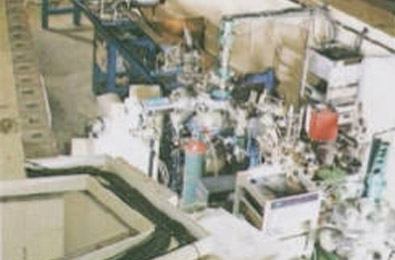
The Inter-University Accelerator Centre Pelletron accelerator along with the low energy ion beam facility (LEIBF) provides a unique opportunity for studies in the field of ion induced materials engineering and characterization. There are two beamlines in the two beamhalls for irradiation studies with accelarated ions from Pelletron and Linac. The beamline in Pelletron beamhall includes two irradiation chambers with on-line ERDA, on-line RGA and ionoluminiscence facilities. Low flux irradiation facility for materials science is also available in another beamline (GPSC). The beamline in Linac beamhall has two irradiation chambers with on-line ERDA and in-situ XRD facility. In-situ Raman facility is also integrated.
Beamlines
- Low flux ion irradiations are perfomed in General Purpose Scattering Chamber (GPSC) beamline.
- Low energy ion irradiations are performed in Low Energy Ion Beam Facility (LEIBF).
Online/Insitu Facilities
Online ERDA
Large area position sensitive gaseous detector telescopes, developed and installed in both the beam halls at IUAC, are used in on-line measurement of SHI induced compositional changes. The detector shown in Fig. (a) is fixed to a 45° port of the high vacuum chamber of materials science beam line in Beam Hall I. The detector offers good Z resolution as shown in Fig. (b) which shows a bi-dimensional ΔE-E recoil spectrum recorded for a silicon oxy-nitride sample. The ΔE1 signal discriminates very well between the recoils of adjacent masses like C, N, O as in this example. The two dimensional position spectra recorded during facility test using 120 MeV Ag ions is shown in Fig. (c). The position sensitivity in scattering plane is around 0.1° which is good enough for correcting the kinematic broadening of the detector (~17% in the present ERD geometry due to the large acceptance of the detector).
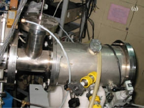
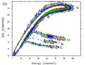
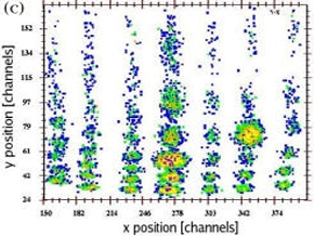
FIG. a) The LAPSDT installed in beam hall I. (b) ΔE1 -E spectrum of recoils from O and N implanted silicon wafer. The spectrum was obtained using 60 MeV Ni5+ projectiles. (c) The xy-position spectrum of fluorine recoils entering the detector after passing through a mask consisting of 49 holes arranged in 7 rows and 7 columns.
Some Publications
- S. A. Khan, Manvendra Kumar, D.K. Avasthi, Development of a position sensitive detector telescope for ERDA based on-line monitoring of swift heavy ions induced modifications, Nucl. Instr. and Meth. B. 266 (2008) 1912
- S. V. S. Nageswara Rao, A. Kothari, G. B. V. S. Lakshmi, S. A. Khan, Ambuj Tripathi, Azher M. Siddiqui, Anand P. Pathak, and D. K. Avasthi, Development of a large area two dimensional position sensitive ΔE-E detector telescope for material analysis, Nucl. Instr. and Meth. B 212 (2003) 545
- Pragya Jain, Ankur Jain, Devendra Vyas, D. Kabiraj, S. A. Khan, and I. P. Jain, Comparative study on hydrogenation properties of Pd capped Mg and Mg/Al films, Int. J. Hydrogen Energy 37 (4) (2012) 37793785
- Yogendra K. Gautam, Amit K. Chawla, Saif A. Khan, R. D. Agrawal, and Ramesh Chandra, Hydrogen absorption and optical properties of Pd/Mg thin films prepared by DC magnetron sputtering, Int. J. Hydrogen Energy 37 (4) (2012) 3772-3778
- Fouran Singh, R. G. Singh, Vinod Kumar, S. A. Khan, and J. C. Pivin, Softening of phonons by lattice defects and structural strain in heavy ion irradiated nanocrystalline zinc oxide films, J. Appl. Phys. 110 (8) (2011) 083520
- S. P. Patel, S. A. Khan, A. K. Chawla, R. Chandra, J. C. Pivin, D. Kanjilal, and L. Kumar, Structural phase diagram for ZnS nanocrystalline thin films under swift heavy ion irradiation, Physica B-Condensed Matter 406 (21) (2011) 4150-4154
- M. Kumar, P. Rajput, S. A. Khan, D. K. Avasthi, A. C. Pandey, Substrate effect on electronic sputtering yield in polycrystalline fluoride (LiF, CaF2 and BaF2 ) thin films, Applied Surface Science 256 (2010) 2199
- Rucha H. Polji, A. D. Yadav, S. K. Dubey, Saif A. Khan, D. K. Avasthi and T. K. Gundu Rao, HI-ERDA, Micro-Raman and HRXRD studies of buried silicon oxynitride layers synthesized by dual ion implantation, Vacuum 83 (2009) 1164
- U. S. Joshi, S. J. Trivedi, K. H. Bhavsar, U. N. Trivedi, S. A. Khan, and D. K. Avasthi, Resistance switching properties of planner Ag/Li:NiO/Ag structures induced by swift heavy ion irradiation, J. of Appl. Phys. 105 (2009) 073704
- Anjali, S. Ghosh, S. A. Khan, P. Srivastava, R. Pal, A. P. Pathak, Study of H loss from hydrogenated Hg1-xCd xTe under high electronic excitation by elastic recoil detection analysis (ERDA), Nucl. Instr. and Meth. B. 267 (2009) 1797
- Sarab Preet Singh, P Srivastava, S Ghosh, Saif A Khan and G Vijaya Prakash, Phase stabilization by rapid thermal annealing in amorphous hydrogenated silicon nitride film, J. Phys.: Condens. Matter 21 (2009) 095010
- D. C. Agarwal, R. S. Chauhan, D. K. Avasthi, S. A. Khan, D. Kabiraj and I. Sulania, Formation of self –affine nanostructures on ZnO surfaces by swift heavy ions, J. Appl. Phys. 104 (2008) 024304
- Y. Batra, S.A. Khan, D. Kabiraj, S. Kumar, D. Kanjilal, Elastic recoil detection (ERD) analysis of GeOx thin films, Nucl. Instr. and Meth. B. 266 (2008) 1697
- Amit Kumar, S. A. Khan, Manvendra Kumar, D. C. Agarwal, Fouran Singh, A. Tripathi, Govind, S. M. Shivaprasad, J. Salomon, L. Pichon, J. C. Pivin and D. K. Avasthi, Oxygen intake in ion irradiated fullerene films, Nucl. Instr. and Meth. B. 266 (2008) 1709.
- A. Tripathi, S.A. Khan, Manvendra Kumar, V. Baranwal, R. Krishna, Sarvesh Kumar, A.C. Pandey, D.K. Avasthi, Angular dependence of electronic sputtering from HOPG, Nucl. Instr. and Meth. B. 266 (2008) 1265
- Shubhra Kala, B. R. Mehta, S. A. Khan, D. K. Avasthi, Nanotracks as transport routes for enhanced and reversible hydrogen diffusion in swift heavy ion irradiated Pd-Pr layers, Appl. Phys. Lett. 90 (2007) 153121
- M. Kumar, S. A. Khan, F. Singh, A Tripathi, D K Avasthi, A C Pandey, Influence of grain size on electronic sputtering of LiF thin films, Nucl. Instr. and Meth. B 256 (2007) 328
- M. Kumar, S. A. Khan, P. Rajput, F. Singh, A. Tripathi, D. K. Avasthi, A. C. Pandey, Size effect on electronic sputtering of LiF thin films, J. Appl. Phys. 102 (2007) 83510
- D. C. Agarwal, R. S. Chauhan, Amit Kumar, D. Kabiraj, F. Singh, S. A. Khan, D. K. Avasthi, J. C. Pivin, M. Kumar, J. Ghatak, and P. V. Satyam, Synthesis and characterization of ZnO thin film grown by electron beam evaporation, J. Appl. Phys. 99 (2006) 123105
- A. Kumar, F. Singh, S. A. Khan, D. C. Agarwal, A. Tripathi, D. K. Avasthi, J. C. Pivin, Precipitation of semiconducting carbon nanoparticles in ion irradiated gels, Nucl. Instr. and Meth. B 244 (2006) 23
- S. Ghosh, V. V. Sivakumar, A. Tripathi, S. Khan, V. Ganesan, A. Gupta, A. Nath, D. K. Avasthi, Formation of nanoscale metallic structures on cupric nitride thin film surface by the impact of 200MeV Au15+ ions, Nucl. Instrum. and Methods in Phys. Res. B 248 (2006) 71
- S. Kumar, R. S. Chauhan, S. A. Khan, W. Bolse, D. K. Avasthi, Swift heavy ion induced mixing in metal/metal system, Nucl. Instr. and Meth. B 244 (2006) 194
- S. Ghosh, D. K. Avasthi, A. Tripathi, D. Kabiraj, P. Sugathan, G. K. Chaudhary, and P. Barua, Heavy ion elastic recoil detection analysis set up for electronic sputtering studies, Rad. Eff. and Defects in Solids 161 (2006) 247
- D. K. Avasthi and W. Assmann, ERDA with swift heavy ions for materials characterization, Current Science 80 (2001) 1532
Ionoluminescence
It is well known that when an ion beam with energy of a few MeV/u impacts on a crystalline or organic specimen, visible light is often observed. This light induced by the energetic ions is termed as Ionoluminescence. IL spectroscopy is a very useful method for understanding material phenomena such as ion matter interaction, impurity characterization, and local symmetry studies. IL can be used not only for characterizing the materials, it can be applied during material modification with ion beams in order to follow the creation of intrinsic defects. Most of the work is planned in view of the applications like new optoelectronic devices, Optical telecommunication, Flat displays (TLD, LCD, LED, ELD) CRT, White LED’s, Lamps & Displays etc.
Some publications
- Determination of the chemical states of impurities in natural Kyanite by the Ionoluminescence technique, H. Nagabhushana, B.Umesh, B.M. Nagabhushana, B.N. Lakshminarasappa, Fouran Singh and R.P.S. Chakradhar, Phil. Mag. 89 (2009) 995.
- Ionoluminescence and Photoluminescence studies of Ag8+ ion irradiated Kyanite, H. Nagabhushana, S.C. Prashantha, B.N. Lakshminarasappa and Fouran Singh, Journal of Luminescence 128 (2008) 7.
- Ion beam-induced luminescence and photoluminescence of 100 MeV Si8+ ion irradiated Kyanite single crystals, H. Nagabhushana, S.C. Prashantha, B.M. Nagabhushana, B.N. Lakshminarasappa, Fouran Singh and R.P.S. Chakradhar, Solid state Communications 147 (2008) 377.
Insitu Micro-Raman Microscope
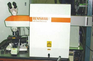
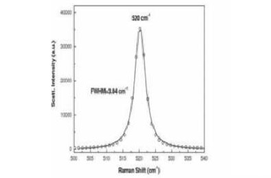
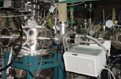
InVia Raman microscope from Renishaw UK has been installed and tested offline in the beam hall-II. The system consists of Ar ion laser with 514.5 nm wavelength and 50 mw power. The Microscope is shown in left figure below. The microscope has very high sensitivity integrated components which enables high resolution confocal measurements. Setup can also support multiple lasers, with automatic software switching of excitation wavelength
Exceptional sensitivity for ultra-low signal detection with minimum noise is possible with compact RenCam CCD detector (105 mm x 105 mm x 135 mm). It is thermoelectrically cooled and operates at -70°C without the need for additional cryogenic coolants and it is deep depletion with UV enhanced coating for future UV excitation applications. The detector is sensitive from 100 to 3200 cm -1 . The integration of the facility the beamline for in-situ measurements is underway.
Online RGA
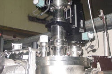
The Pfeiffer QMA 422 quadrupole mass analyzer system with SIMS option (under IRHPA programme of DST) operating at 2.25 MHz and can mass analyze in the range 1-1024 amu with mass separation (ΔM/M) better than 0.01 is installed in materials science beamline. The QMA has a 3 lens optics The facility is used for on line detection of release of gases, specially from polymers and online study of electronic sputtering. The QMS is attached to a 90° port of ultra-high vacuum (UHV) chamber. The probe consisting of 3 lens optics for detecting both positive and negative ions as well as neutral atoms is nearly 5 mm from the sample surface during the measurements.
Recent Publications
- G. B. V. S. Lakshmi, Jai Prakash, S. A. Khan, Azher M. Siddiqui, and M. Zulfequar, Modifications induced by swift heavy ion beam of 60 MeV Si5+ in Poly(3-octylthiophene), Science of Advanced Materials 4 (2012) 1024-1030.
- K. Sangeetha, R. Ramesh Babu, K. Ramamurthi, Jai Prakash, and S. A. Khan, Spectral studies on Ag8+ ions irradiated LAHCl.H2O and LAHBr.H2O single crystals, Spectrochemica Acta Part A 79 (2011) 884-888.
- G. B. V. S. Lakshmi, D. K. Avasthi, Jai Prakash, Azher M. Siddiqui, Vazid Ali, S. A. Khan, and M. Zulfequar, Structural, optical and gas evolution studies of 60 MeV Si5+ ion irradiated PoT-PVC blends, Adv. Mat. Lett. 2(2) (2011) 125-130
- Jai Prakash, A. Tripathi, S. A. Khan, J. C. Pivin, F. Singh, Jalaj Tripathi, Sarvesh Kumar, and D. K. Avasthi, Ion beam induced interface mixing of Ni on PTFE bilayer system studied by quadrupole mass analysis and electron spectroscopy for chemical analysis, Vacuum 84(11) (2010) 1275-1279.
Insitu XRD
Contact Persons : P. K. Kulriya, pawan@iuac.res.in
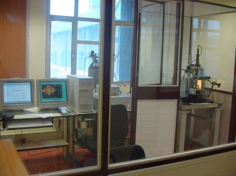
X-Ray diffraction analysis (XRD) is the primary tool to investigate the structure of crystalline materials. An in situ x-ray diffraction (XRD) has been setup in the materials science beam line of Pelletron accelerator. It is mainly used for in situ studies of phase change in swift heavy ion (SHI) irradiation. The advanced D-8 x-ray diffractometer (acquired from Bruker AXS Germany) is installed in beamhall-II under IRHPA programme of Department of Science and Technology (DST), Govt. of India. Generally, there are variations from sample to sample in the synthesis of nanoparticles and thin films, and the effect of ion irradiation depends on the initial state of the sample. Therefore, it becomes desirable that the ion fluence dependent study should be performed on the same sample. The in- situ XRD facility allows studying the XRD of the same sample at various fluence to understand the influence of swift heavy ion irradiation. There are some materials which show phase transformation when irradiated with SHI at low temperature. To study such a system, low temperature (LN2) in situ XRD study is essential. Therefore, a low temperature cooling setup is also installed. This setup is also used as a standard off-line diffractometer at low temperature and room temperature when there is no beam from the accelerator. The work is in progress to interface a CCR to bring down the sample temperature to 20 K (supported by nano mission project of DST).
![A photograph of the in situ x-ray diffraction setup with its sample cooling unit [1] A photograph of the in situ x-ray diffraction setup with its sample cooling unit [1]](http://iuac.res.in/themes/iuac/images/xrd-img-1.jpg)
A photograph of the whole in-situ x-ray diffraction setup with its sample cooling unit at the materials science beam line at IUAC is shown in figure 1. Normally, the model has a vertically mounted goniometer having the sample in the horizontal plane. Since the ion beam is incident in the vertical plane, the samples mount needs to be vertical; therefore, the diffractometer is modified accordingly by Bruker. Chamber is designed and fabricated to interface with the base of goniometer and the beamline. An adapter vacuum flange is inserted to couple the chamber with the base of goniometer. This instrument equipped with a Cu Kα conventional x-ray source, Göbble mirror, LiF monochromator, scintillator detector. The facility is also equipped with a high speed position sensitive detector besides conventional NaI(Tl) scintillation counter. It is about to 60 times faster as compared to scintillation counter with reasonably good resolution. This detector is very useful for in-situ ion irradiation experiments, where fast scanning is required to optimize the utilization of accelerator time. The detailed specifications of the instrument are given in ref. 1. The XRD setup is used by many researchers for insitu as well as offline XRD analysis.
Following are the highlight of some of the interesting results that came out from IUAC diffractometer.
Case 1: Low temperate ion irradiation induced insitu XRD analysis
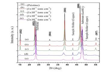
Low temperature ion irradiation induced structural modification in YBa2Cu3O7-y thin films: An in situ x-ray diffraction study [J. of Appl. Phys. 106 (2009)053912]
The in situ x-ray diffraction (XRD) study of 200 MeV Ag ion irradiation induced structural modification in c-axis oriented YBa2Cu3O7-y (YBCO) thin films at 89 K is carried out [2]. Figure 2 shows the evolution of low temperature (T=89 K) in situ XRD pattern of an YBa2Cu3O7-y thin film with 200 MeV Ag ion irradiation. It is observed that the films remained c-axis oriented up to a fluence of 2x10¹³ ions cm−2, where complete amorphization occurs. This observation is explained on the basis of SHI induced secondary electrons, which create oxygen disorder by an electron capture process in the CuO chains of a fully oxygenated YBCO structure. The FWHM of XRD peaks and the microstrain around ion tracks showed an incubation effect up to a fluence of 1x10¹² ions cm−2, and subsequently these parameters increased due to the proximity of strained regions around ion tracks. This study suggested that SHI induces three different types of defects in YBCO at LT: (i) amorphous ion tracks provided Se>Se th, (ii) strained region around ion track, and (iii) oxygen disorder (point defects) in the CuO basal plane.
Case 2: Low temperature insitu XRD analysis of the samples in controlled gas atmosphere
Hydrogen induced structural modification in palladium nanoparticles [J. Appl. Phys. 106 (2009)093515]
A detailed structural study involving in-situ XRD analysis carried out on Pd nanoparticle and thin film samples at hydrogen concentrations of 2, 5 and 10% over temperature ranging from -100°C to 55°C and hydrogen pressures ranging from 250-1000 mbar(Fig. 3). Variation in lattice constant has been interpreted in terms of hydrogen content in α and β PdHx phases and decrease in XRD peak intensity has been interpreted in terms of hydrogen induced degradation in crystalline quality and temperature induced lattice disorder. It is observed that Pd-H interaction is strongly influenced by the temperature and pressure dependences of physisorption, chemisorption and diffusion. These results show that the increased surface area, interparticle gaps, electronic enhancement result in enhanced Pd-H interaction in case of nanoparticles. In addition, presence of single β phase and lower crystallinity degradation is observed in case of Pd nanoparticles in comparison to thin films. The above mentioned differences between nanoparticles and thin films are more pronounced at lower temperatures due to the increased presence of subsurface sites pronounced at lower temperatures due to the increased presence of subsurface sites.
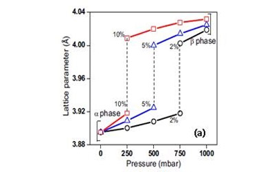
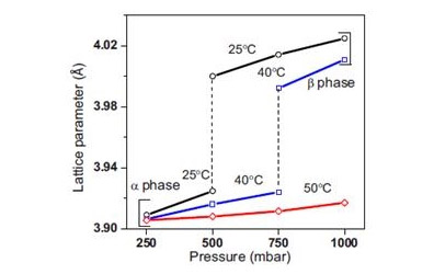
Fig:3 (a) Relationship between the lattice constant and "steady state" pressure during hydrogen adsorption at Tm=25 °C and Hc=2%, 5%, and 10% and (b) relationship between the lattice constant and steady and state pressure during hydrogen adsorption at Tm=25, 40, and 50 °C and Hc=5% for the for the Pd nanoparticles sample.
Case 3: In-situ monitoring of growth of Au nanoparticles under SHI
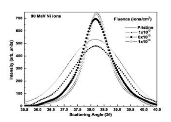
Controlled growth of gold nanoparticles induced by ion irradiation: An in situ x-ray diffraction study [Appl. Phys. Lett., 90 (2007) 073110]
The insitu XRD facility was used to study the growth of Au nanoparticles due to swift heavy ion irradiation. Thin films of silica having thickness of about to 100 nm containing Au nanoparticles were deposited on quartz by atom beam sputtering process. The samples were irradiated at normal beam incidence with ion fluence varying from 1x10¹³ to 1x10¹⁴ ions cm-2 using the 15UD Pelletron accelerator at the Inter University Accelerator Centre, New Delhi. The XRD spectra (Fig 4) of the sample recorded after every fluence of 2x10¹³ ions cm-2 using a high speed position sensitive Vantec detector. A significant growth in Au nanoparticle size (from 4 to 9 nm) is observed on irradiation with 90 MeV Ni to a fluence of 1x10¹⁴ ions cm-2 , as confirmed from in-situ XRD, UV-visible absorption, and TEM measurement data. There is also a decrease in lattice constant with ion fluence, which signifies the growth of Au nanoparticles on the ion irradiation. The work demonstrated that SHI is a good tool for tailoring the size of particle, and hence the optical properties of metal nanoparticles.
References
- Setup for insitu X-ray diffractometer study of swift heavy ion irradiated materials, P. K. Kulriya, F. Singh, A. Tripathi, R. Ahuja, A. Kothari, R. N. Dutt, Y. K. Mishra, Amit Kumar, D. K. Avasthi, Review of Scientific Instrument 78 (2007) 113901
- 200 MeV silver ion irradiation induced structural modification in YBa2Cu3O7-y thin films at 89 K: An in situ x-ray diffraction study, R. Biswal, J. John, P. Mallick, B. N. Dash, P. K. Kulriya, D. K. Avasthi, D. Kanjilal, D. Behera, T. Mohanty, P. Raychaudhuri, and N. C. Mishra, Journal of Applied Physics 106, 053912 (2009)
- Hydrogen induced lattice expansion and crystallinity degradation in palladium nanoparticles: Effect of hydrogen concentration, pressure, and temperature, Manika Khanuja, B. R. Mehta, Pragya Agar, P. K. Kulriya, and D. K. Avasthi, J. Appl. Phys. 106 (2009) 093515
- Controlled growth of gold nanoparticles induced by ion irradiation: An in situ x-ray diffraction study, Y. K. Mishra, D. K. Avasthi, P. K. Kulriya, F. Singh, D. Kabiraj, and A. Tripathi, J. C. Pivin, I. S. Bayer and A. Biswas, Appl. Phys. Lett., 90 (2007) 073110
Offline Facilities
The available characterizations of semiconductors and oxides before and after ion beam irradiation and implantation are:
- Temperature dependent resistivity (R-T)
- Isothermal current-voltage (I-V) and
- Capacitance-voltage (C-V) characteristics
Apart from this one can do dielectric measurements in the range of 20 Hz to 1 MHz. There are opportunities for users to develop other measurements like Hall Effect, magnetoresistance set up, vibrating sample magnetometer using the infrastructure available in the laboratory. At present, one can do measurements from ~80 K to 400 K and in near future it should be possible to do measurements down to ~10K. Above experimental setups are interfaced using GPIB with PC.
No content available
Insitu Micro-Raman Microscope
InVia Raman microscope from Renishaw UK has been installed and tested offline in the beam hall-II. The system consists of Ar ion laser with 514.5 nm wavelength and 50 mw power. The Microscope is shown in left figure below. The microscope has very high sensitivity integrated components which enables high resolution confocal measurements. Setup can also support multiple lasers, with automatic software switching of excitation wavelength
Exceptional sensitivity for ultra-low signal detection with minimum noise is possible with compact RenCam CCD detector (105 mm x 105 mm x 135 mm). It is thermoelectrically cooled and operates at -70°C without the need for additional cryogenic coolants and it is deep depletion with UV enhanced coating for future UV excitation applications. The detector is sensitive from 100 to 3200 cm -1 . The integration of the facility the beamline for in-situ measurements is underway.
No content available
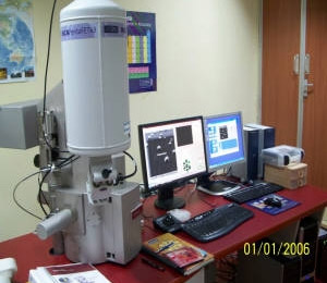
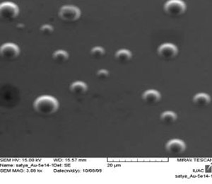
A field emission scanning electron microscope (FE-SEM): MIRA II LMH from TESCAN, with a resolution of 1.5 nm at 30 kV has been installed to boost research activities in nanomaterials, in a project funded under Nano Initiative program of Department of Science and Technology. It has a secondary electron (SE) and a backscattered electron (BSE) detector for imaging. An energy dispersive X ray detector INCA PentaFET3 with 133 eV resolution from OXFORD has also been installed in this system for elemental analysis.
Sputter Coater System for FE-SEM
To improve the performance and applicability to different types of samples, Q150T-S High Vacuum Turbo pumped Sputter Coater system from Quoram Technologies has been installed. The system is regularly being used to coat the samples with gold, carbon and chromium.
The SEM facility is being heavily utilized for characterization of samples of IUAC users. The list of publications which benefited from this facility are listed below.
2017
- A. Das, S.K. Gautam, D.K. Shukla, F. Singh, Correlations of charge neutrality level with electronic structure and p-d hybridization, Scientific Reports, 7 (2017) 40843.
- B.A. Malik, M.A. Malik, K. Asokan, Enhancement of the critical current density in YBCO/Ag composites, Chinese Journal of Physics, 55 (2017) 170-175.
2016
- M. Bala, R. Meena, S. Gupta, C. Pannu, T.S. Tripathi, S. Varma, S.K. Tripathi, K. Asokan, D.K. Avasthi, Formation of nanodots and enhancement of thermoelectric power induced by ion irradiation in PbTe:Ag composite thin films, Nuclear Instruments and Methods in Physics Research Section B: Beam Interactions with Materials and Atoms, 379 (2016) 36-41.
- M. Gupta, P.K. Kulriya, R. Shukla, R.S. Dhaka, R. Kumar, S.S. Ghumman, Reduction and structural modification of zirconolite on He+ ion irradiation, Nuclear Instruments and Methods in Physics Research Section B: Beam Interactions with Materials and Atoms, 379 (2016) 119-125.
- Z. Habib, K. Majid, M. Ikram, K. Sultan, S.A. Mir, K. Asokan, Influence of Ni substitution at B-site for Fe3+ ions on morphological, optical, and magnetic properties of HoFeO3 ceramics, Applied Physics A, 122 (2016) 550.
- S. Hooda, S.A. Khan, B. Satpati, D. Kanjilal, D. Kabiraj, Thermal spike effect in sputtering of porous germanium to form surface pattern by high energy heavy ions irradiation, Applied Physics Letters, 108 (2016) 201603.
- S. Hooda, S.A. Khan, B. Satpati, D. Stange, D. Buca, M. Bala, C. Pannu, D. Kanjilal, D. Kabiraj, Effect of ion beam parameters on engineering of nanoscale voids and their stability under post-growth annealing, Applied Physics A, 122 (2016) 227.
- S. Hooda, S.A. Khan, B. Satpati, A. Uedono, S. Sellaiyan, K. Asokan, D. Kanjilal, D. Kabiraj, Nanopores formation and shape evolution in Ge during intense ionizing irradiation, Microporous and Mesoporous Materials, 225 (2016) 323-330.
- K. Joshi, M. Rawat, S.K. Gautam, R.G. Singh, R.C. Ramola, F. Singh, Band gap widening and narrowing in Cu-doped ZnO thin films, Journal of Alloys and Compounds, 680 (2016) 252-258.
- M. Kalidasan, K. Asokan, R. Dhanasekaran, Luminescence properties of 100 MeV W8+ ion irradiated GdCa4O(BO3)3:Eu3+ and GdCa4O(BO3)3:Tb3+ phosphors, Journal of Luminescence, 180 (2016) 241-250.
- M. Kumar, P. Rajput, P.K. Singh, A.C. Yadav, S.A. Khan, S.N. Jha, F. Singh, A.C. Pandey, Europium activated gadolinium sulfide nanoparticles, RSC Advances, 6 (2016) 108523-108529.
- P. Kumar, P. Kumar, A. Kumar, R.C. Meena, R. Tomar, F. Chand, K. Asokan, Structural, morphological, electrical and dielectric properties of Mn doped CeO2, Journal of Alloys and Compounds, 672 (2016) 543-548.
- H.S. Lokesha, K.R. Nagabhushana, F. Singh, Enhancement in luminescence properties of ZrO2:Dy3+ under 100 MeV swift Ni7+ ion irradiation, RSC Advances, 6 (2016) 55240-55247.
- B.A. Malik, M.A. Malik, K. Asokan, Optimization of BaZrO3 concentration as secondary phase in superconducting YBa2Cu3O7 for high current applications, AIP Advances, 6 (2016) 045317.
- M.P.S. Rana, F. Singh, K. Joshi, S. Negi, R.C. Ramola, Influence of electronic excitations on structural, optical and electrical properties of undoped and antimony doped tin oxide thin films, Thin Solid Films, 616 (2016) 34-42.
- M.P.S. Rana, F. Singh, S. Negi, S.K. Gautam, R.G. Singh, R.C. Ramola, Band gap engineering and low temperature transport phenomenon in highly conducting antimony doped tin oxide thin films, Ceramics International, 42 (2016) 5932-5941.
- N.J. Shivaramu, B.N. Lakshminarasappa, K.R. Nagabhushana, F. Singh, Effect of 100 MeV swift Si8+ ions on structural and thermoluminescence properties of Y2O3:Dy3+nanophosphor, Radiation Effects and Defects in Solids, 171 (2016) 408-420.
- U.B. Singh, S.K. Gautam, S. Kumar, S. Hooda, S. Ojha, F. Singh, Ion beam induced optical and surface modification in plasmonic nanostructures, Nuclear Instruments and Methods in Physics Research Section B: Beam Interactions with Materials and Atoms, 379 (2016) 42-47.
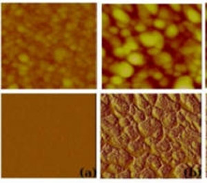
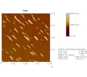
Multi Mode SPM with Nanoscope IIIa controller acquired from Digital/Veeco Instruments Inc. (under IRHPA programme of DST) is extensively used in all the modes in user experiments. All SPM modes are used in experiments : AFM, MFM, C-AFM, STM, STS and F-d mode etc. PSD studies for surface growth and Force-Distance studies are also done.
The formation of conducting tracks in fullerene films after irradiation with 120 MeV Au ions by Conducting AFM are shown in figure(a) Besides this, swift heavy ion induced magnetization in C60 films by MFM has also been observed as shown in fig (b).
- Transmission Electron Microscopy www.targetiuac.wixsite.com
Insitu XRD
Contact Persons : P. K. Kulriya, pawan@iuac.res.in
X-Ray diffraction analysis (XRD) is the primary tool to investigate the structure of crystalline materials. An in situ x-ray diffraction (XRD) has been setup in the materials science beam line of Pelletron accelerator. It is mainly used for in situ studies of phase change in swift heavy ion (SHI) irradiation. The advanced D-8 x-ray diffractometer (acquired from Bruker AXS Germany) is installed in beamhall-II under IRHPA programme of Department of Science and Technology (DST), Govt. of India. Generally, there are variations from sample to sample in the synthesis of nanoparticles and thin films, and the effect of ion irradiation depends on the initial state of the sample. Therefore, it becomes desirable that the ion fluence dependent study should be performed on the same sample. The in- situ XRD facility allows studying the XRD of the same sample at various fluence to understand the influence of swift heavy ion irradiation. There are some materials which show phase transformation when irradiated with SHI at low temperature. To study such a system, low temperature (LN2) in situ XRD study is essential. Therefore, a low temperature cooling setup is also installed. This setup is also used as a standard off-line diffractometer at low temperature and room temperature when there is no beam from the accelerator. The work is in progress to interface a CCR to bring down the sample temperature to 20 K (supported by nano mission project of DST).
![A photograph of the in situ x-ray diffraction setup with its sample cooling unit [1] A photograph of the in situ x-ray diffraction setup with its sample cooling unit [1]](http://iuac.res.in/themes/iuac/images/xrd-img-1.jpg)
A photograph of the whole in-situ x-ray diffraction setup with its sample cooling unit at the materials science beam line at IUAC is shown in figure 1. Normally, the model has a vertically mounted goniometer having the sample in the horizontal plane. Since the ion beam is incident in the vertical plane, the samples mount needs to be vertical; therefore, the diffractometer is modified accordingly by Bruker. Chamber is designed and fabricated to interface with the base of goniometer and the beamline. An adapter vacuum flange is inserted to couple the chamber with the base of goniometer. This instrument equipped with a Cu Kα conventional x-ray source, Göbble mirror, LiF monochromator, scintillator detector. The facility is also equipped with a high speed position sensitive detector besides conventional NaI(Tl) scintillation counter. It is about to 60 times faster as compared to scintillation counter with reasonably good resolution. This detector is very useful for in-situ ion irradiation experiments, where fast scanning is required to optimize the utilization of accelerator time. The detailed specifications of the instrument are given in ref. 1. The XRD setup is used by many researchers for insitu as well as offline XRD analysis.
Following are the highlight of some of the interesting results that came out from IUAC diffractometer.
Case 1: Low temperate ion irradiation induced insitu XRD analysis

Low temperature ion irradiation induced structural modification in YBa2Cu3O7-y thin films: An in situ x-ray diffraction study [J. of Appl. Phys. 106 (2009)053912]
The in situ x-ray diffraction (XRD) study of 200 MeV Ag ion irradiation induced structural modification in c-axis oriented YBa2Cu3O7-y (YBCO) thin films at 89 K is carried out [2]. Figure 2 shows the evolution of low temperature (T=89 K) in situ XRD pattern of an YBa2Cu3O7-y thin film with 200 MeV Ag ion irradiation. It is observed that the films remained c-axis oriented up to a fluence of 2x10¹³ ions cm−2, where complete amorphization occurs. This observation is explained on the basis of SHI induced secondary electrons, which create oxygen disorder by an electron capture process in the CuO chains of a fully oxygenated YBCO structure. The FWHM of XRD peaks and the microstrain around ion tracks showed an incubation effect up to a fluence of 1x10¹² ions cm−2, and subsequently these parameters increased due to the proximity of strained regions around ion tracks. This study suggested that SHI induces three different types of defects in YBCO at LT: (i) amorphous ion tracks provided Se>Se th, (ii) strained region around ion track, and (iii) oxygen disorder (point defects) in the CuO basal plane.
Case 2: Low temperature insitu XRD analysis of the samples in controlled gas atmosphere
Hydrogen induced structural modification in palladium nanoparticles [J. Appl. Phys. 106 (2009)093515]
A detailed structural study involving in-situ XRD analysis carried out on Pd nanoparticle and thin film samples at hydrogen concentrations of 2, 5 and 10% over temperature ranging from -100°C to 55°C and hydrogen pressures ranging from 250-1000 mbar(Fig. 3). Variation in lattice constant has been interpreted in terms of hydrogen content in α and β PdHx phases and decrease in XRD peak intensity has been interpreted in terms of hydrogen induced degradation in crystalline quality and temperature induced lattice disorder. It is observed that Pd-H interaction is strongly influenced by the temperature and pressure dependences of physisorption, chemisorption and diffusion. These results show that the increased surface area, interparticle gaps, electronic enhancement result in enhanced Pd-H interaction in case of nanoparticles. In addition, presence of single β phase and lower crystallinity degradation is observed in case of Pd nanoparticles in comparison to thin films. The above mentioned differences between nanoparticles and thin films are more pronounced at lower temperatures due to the increased presence of subsurface sites pronounced at lower temperatures due to the increased presence of subsurface sites.


Fig:3 (a) Relationship between the lattice constant and "steady state" pressure during hydrogen adsorption at Tm=25 °C and Hc=2%, 5%, and 10% and (b) relationship between the lattice constant and steady and state pressure during hydrogen adsorption at Tm=25, 40, and 50 °C and Hc=5% for the for the Pd nanoparticles sample.
Case 3: In-situ monitoring of growth of Au nanoparticles under SHI

Controlled growth of gold nanoparticles induced by ion irradiation: An in situ x-ray diffraction study [Appl. Phys. Lett., 90 (2007) 073110]
The insitu XRD facility was used to study the growth of Au nanoparticles due to swift heavy ion irradiation. Thin films of silica having thickness of about to 100 nm containing Au nanoparticles were deposited on quartz by atom beam sputtering process. The samples were irradiated at normal beam incidence with ion fluence varying from 1x10¹³ to 1x10¹⁴ ions cm-2 using the 15UD Pelletron accelerator at the Inter University Accelerator Centre, New Delhi. The XRD spectra (Fig 4) of the sample recorded after every fluence of 2x10¹³ ions cm-2 using a high speed position sensitive Vantec detector. A significant growth in Au nanoparticle size (from 4 to 9 nm) is observed on irradiation with 90 MeV Ni to a fluence of 1x10¹⁴ ions cm-2 , as confirmed from in-situ XRD, UV-visible absorption, and TEM measurement data. There is also a decrease in lattice constant with ion fluence, which signifies the growth of Au nanoparticles on the ion irradiation. The work demonstrated that SHI is a good tool for tailoring the size of particle, and hence the optical properties of metal nanoparticles.
References
- Setup for insitu X-ray diffractometer study of swift heavy ion irradiated materials, P. K. Kulriya, F. Singh, A. Tripathi, R. Ahuja, A. Kothari, R. N. Dutt, Y. K. Mishra, Amit Kumar, D. K. Avasthi, Review of Scientific Instrument 78 (2007) 113901
- 200 MeV silver ion irradiation induced structural modification in YBa2Cu3O7-y thin films at 89 K: An in situ x-ray diffraction study, R. Biswal, J. John, P. Mallick, B. N. Dash, P. K. Kulriya, D. K. Avasthi, D. Kanjilal, D. Behera, T. Mohanty, P. Raychaudhuri, and N. C. Mishra, Journal of Applied Physics 106, 053912 (2009)
- Hydrogen induced lattice expansion and crystallinity degradation in palladium nanoparticles: Effect of hydrogen concentration, pressure, and temperature, Manika Khanuja, B. R. Mehta, Pragya Agar, P. K. Kulriya, and D. K. Avasthi, J. Appl. Phys. 106 (2009) 093515
- Controlled growth of gold nanoparticles induced by ion irradiation: An in situ x-ray diffraction study, Y. K. Mishra, D. K. Avasthi, P. K. Kulriya, F. Singh, D. Kabiraj, and A. Tripathi, J. C. Pivin, I. S. Bayer and A. Biswas, Appl. Phys. Lett., 90 (2007) 073110
Synthesis Facilities
Evaporator-II
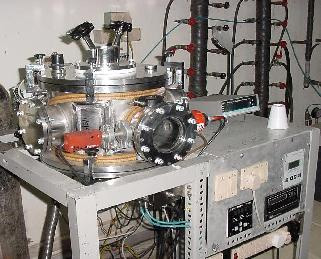
Features
- Resistive heating arrangement.
- Quartz crystal thickness monitor.
- Pumped by turbo molecular pump.
- A wide beam ion gun to sputter clean substrate.
- Substrate cooling upto 100K.
- Base pressure ~10-7 mbar.
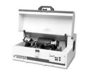
A SPEX CertiPrep 8000D Dual Mixer/Mill has been installed and used for synthesis of nanopowder materials. Hardened steel, Agate and Silicon Nitride vials are available for pulverizing Ferrite and semiconductor materials. This system can also be used for mechanical alloying of powder materials. Nanopowders of Mn0.4Zn0.6Fe2O4, Bi doped BaS, Ce doped SrS, Y3Fe5O12, SiO2 were prepared by pulverizing their powder materials and nanopowders of Boron-Carbon-Nitride (BN + Graphite ) and SiC (Si + Graphite ) were prepared by mechanical alloying.
No content available
A Multi-target DC sputtering system has been assembled and used for thin film deposition from metal targets. The system includes :
- DC power supply : 2 kW, ( 1000 V, 2 A).
- Stainless steel deposition chamber with water cooled target holders (3 Nos) for 2 inch diameter targets and view ports.
- Vacuum system : Turbo pump used to produce high vacuum, Penning and Pirani gauges used to measure the vacuum.
- Gas flow : MKS MFC used to feed gas at controlled rate.
- Manual gate valve used as throttle valve to set the deposition pressure.
- Substrate heater with heating upto 750oC and having rotation provision for film uniformity.
Argon and oxygen gases can be used to grow thin films of metals and metal-oxides using metal targets of 2 inch diameter. Thin films of Fe were grown to test the system and the films were deposited at 4 nm/min deposition rate at 80 W power.
Evaporator-I
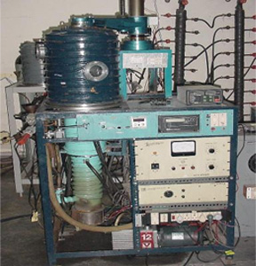
Features:
- Resistive heating arrangement.
- A single pocket electron beam gun and 2kW power supply.
- Quartz crystal thickness monitor.
- Pumped by a diffusion pump with liquid nitrogen trap.
- Base pressure ~10-7 mbar.
Cryo pump based HV evaporator
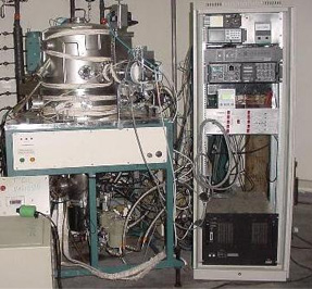
A cryo-pump based HV evaporator has been setup to prepare thin films under hydrocarbon free high vacuum condition. It is used extensively for the preparation of thin film multi-layers for materials science experiments, targets of metals of high melting point with low vapour pressure and various other applications which require hydrocarbon free evaporation environment.
Evaporation source:
A 4-pocket electron gun and 6 kW power supply.
Resistive heating arrangement.
Online thickness measurement:
Dual crystal thickness monitor.
Programmable deposition controller.
The electron gun power supply is interface to this controller which controls the output power of the e-gun by PID method according to the programmed deposition schedule.
The thickness of a film can be defined within an accuracy of 1 Å and the rate of deposition can be controlled with accuracy of 0.1 Å/s.
Pumping station:
- Scroll pump (for roughing of evaporator and backing of turbo molecular pump).
- Turbo molecular pump.
- Cryo pump.
Base pressure is 2x10⁻⁸ mbar.
Substrate heater:
Heating upto 400oC.
Residual Gas Analyze (RGA):
Pfeiffer Prisma QMS200, 200amu RGA installed to monitor partial pressure of gases in the evaporator.
A thermal evaporation set-up was assembled and used for thin film deposition using Al foil. The system includes :
- Turbo pump/ Dry pump based vacuum pumping system.
- Resistive heating set up consisting of 300 mm Dia 350 mm High water cooled SS Bell Jar with 70 mm Dia view ports (2 Nos), High Current Voltage power supply LT Transformer ( 200 amps/8 V), LT feedthroughs and source holder.
- Penning and Pirani gauges used to measure the vacuum.
The system was tested by depositing a uniform Al film on glass slide.
No content available
An indigenously developed rf sputtering system is being used regularly for the deposition of thin films. The system includes:
- RF power supply: Indigenously developed 500 W, 13.56 MHz with matching network.
- Stainless steel deposition chamber with water cooled target holders for 2 inch and 4 inch diameter targets, grounded anode, view port, and ports for vacuum components, gas flow, shutter and electrical feedthroughs.
- Vacuum system: Turbo pump/Dry pump used to produce clean vacuum, Penning and pirani gauges used for measuring the vacuum.
- Gas flow: MKS MFC’s used to feed gas into the chamber at set flow rates.
- Manual gate valve used as throttle valve to set the deposition pressure in combination with the gas flow rates.
- Substrate heater: 2 inch diameter substrate holder with K type Thermocouple, radiation shield and heating upto 600°C.
Argon, Oxygen and nitrogen gases can be used to grow thin films of metals, oxides and nitrides. Thin films of ZnO, ZnO/SiOx nanocomposites, ZnS, ZnS/SiOx nanocomposite, Ni, Mg-Mn Ferrites, Strontium Barium Niobate, CeO2 , Hydroxyapatite, Copper nitride, Boron-Carbon-Nitride etc. have been synthesized for performing ion beam irradiation studies.
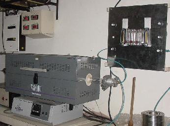
- Annealing at temperature upto 10000C.
- A 8 ramp 8 dwell multi programmable controller.
- Annealing in controlled atmosphere inside quartz tube.


![The evolution of fluorine and various fluorocarbon gases during the ion irradiation of Ni-PTFE system is shown in figure above [Jai Prakash et al., Vacuum 84 (2010) 1275]. The evolution of fluorine and various fluorocarbon gases during the ion irradiation of Ni-PTFE system is shown in figure above [Jai Prakash et al., Vacuum 84 (2010) 1275].](http://iuac.res.in/themes/iuac/images/rga-img-thumb-2.jpg)
![Gel Electrophoresis [Stratagene, Tarson], AFIGE [BIORAD], Semi Dry Blotter [BIORAD], PCR [Perkin Elmer] Gel Electrophoresis [Stratagene, Tarson], AFIGE [BIORAD], Semi Dry Blotter [BIORAD], PCR [Perkin Elmer]](http://iuac.res.in/themes/iuac/images/uvvis-img-thumb-1.jpg)
![UV Vis Spectrophotometer [Hitachi] UV Vis Spectrophotometer [Hitachi]](http://iuac.res.in/themes/iuac/images/uvvis-img-thumb-2.jpg)
![PCR [Applied Biosystems] PCR [Applied Biosystems]](http://iuac.res.in/themes/iuac/images/uvvis-img-thumb-3.jpg)
![96 Well Multi Mode Plate Reader [Perkin Elmer, Victor X5] 96 Well Multi Mode Plate Reader [Perkin Elmer, Victor X5]](http://iuac.res.in/themes/iuac/images/uvvis-img-thumb-4.jpg)
![Centrifuge [Eppendorf] Centrifuge [Eppendorf]](http://iuac.res.in/themes/iuac/images/uvvis-img-thumb-5.jpg)
![Fluorescence Microscope [Zeiss] Fluorescence Microscope [Zeiss]](http://iuac.res.in/themes/iuac/images/uvvis-img-thumb-6.jpg)